Lithographic apparatus and device manufacturing method

a technology of lithographic apparatus and manufacturing method, which is applied in the direction of electrical apparatus, printers, instruments, etc., can solve the problems achieve the effect of reducing the effect of thin film interference on signal strength, more robustness, and effective average out certain errors

Inactive Publication Date: 2005-01-20
ASML NETHERLANDS BV
View PDF17 Cites 14 Cited by
  • Summary
  • Abstract
  • Description
  • Claims
  • Application Information

AI Technical Summary

Benefits of technology

[0018] The use of an imaging system capable of imaging at least two wavelengths correctly onto a single image plane is advantageous in that it is more robust than single wavelength alignment. The use of multiple colors effectively averages out certain errors in the alignment signal due to asymmetric marks and the detection at one single imaging plane makes it unnecessary to mix the detection single of the two distinct wavelengths. Furthermore it diminishes the effect of thin film interference effects on signal strength. Both a true broadband spectrum and a set of discrete (laser) wavelengths may

Problems solved by technology

Furthermore it diminishes the effect of thin

Method used


Image

  • Lithographic apparatus and device manufacturing method
  • Lithographic apparatus and device manufacturing method
  • Lithographic apparatus and device manufacturing method

Examples


Embodiment Construction

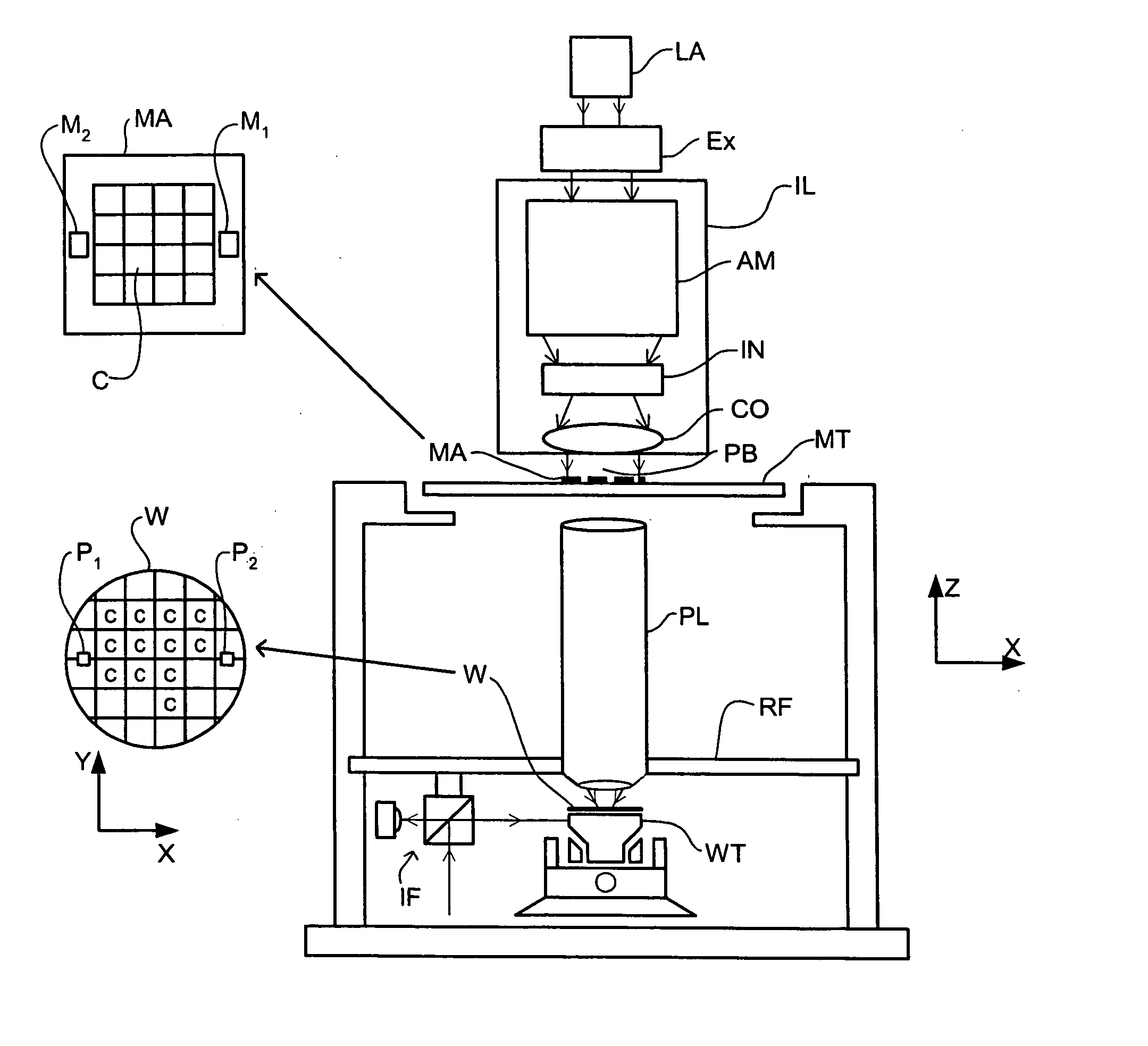
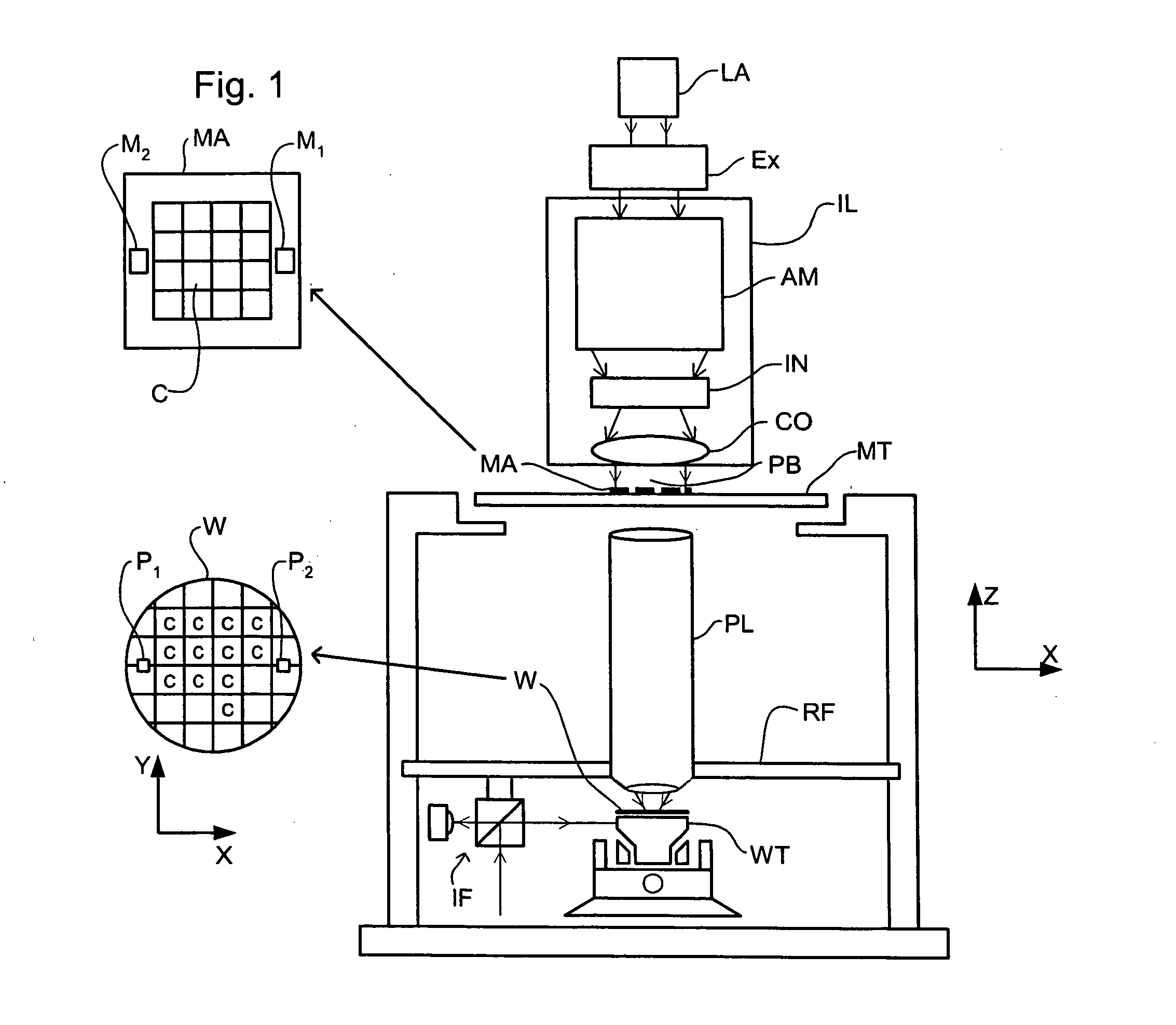
[0037]FIG. 1 schematically depicts a lithographic projection apparatus according to a particular embodiment of the invention. The apparatus includes a radiation system Ex, IL that supplies a projection beam PB of radiation (e.g. UV or EUV radiation). In this embodiment, the radiation system also comprises a radiation source LA; a first object table (mask table) MT provided with a mask holder for holding a mask MA (e.g. a reticle), and connected to a first positioning device M1, M2 to accurately position the mask with respect to a projection system PL; a second object table (substrate table) WT provided with a substrate holder for holding a substrate W (e.g. a resist-coated silicon wafer), and connected to a second positioning device P1, P2 to accurately position the substrate with respect to the projection system PL; the projection system (“lens”) PL (e.g. a refractive or catadioptric system, a mirror group or an array of field deflectors) constructed and arranged to image an irradi...


PUM


Abstract

An off-axis alignment system in a lithographic projection apparatus uses broadband radiation to illuminate a phase grating on the wafer. The broadband radiation source may include fluorescent materials, e.g. Yag:Ce or ND:Yag crystals illuminated by excitation light.

Description

BACKGROUND OF THE INVENTION [0001] 1. Field of the Invention [0002] The present invention relates to a lithographic projection apparatus. [0003] 2. Description of the Related Art [0004] The term “patterning device” as here employed should be broadly interpreted as referring to device that can be used to endow an incoming radiation beam with a patterned cross-section, corresponding to a pattern that is to be created in a target portion of the substrate. The term “light valve” can also be used in this context. Generally, the pattern will correspond to a particular functional layer in a device being created in the target portion, such as an integrated circuit or other device (see below). An example of such a patterning device is a mask. The concept of a mask is well known in lithography, and it includes mask types such as binary, alternating phase-shift, and attenuated phase-shift, as well as various hybrid mask types. Placement of such a mask in the radiation beam causes selective tra...

Claims


Application Information

Patent Timeline
IPC IPC(8): G03F9/00G03F7/20H01L21/027
CPCG03F9/7049G03F9/7088G03F9/7076G03F7/20
Inventor NEIJZEN, JACOBUS HERMANUS MARIAMONSHOUWER, RENE
Owner ASML NETHERLANDS BV
Why Eureka
Try Eureka