Semiconductor laser module having a co-axial package and transmission lines for complementary driving signal

a technology of complementary driving signal and laser module, which is applied in the direction of semiconductor laser, optical elements, instruments, etc., can solve the problems of degrading achieve the effect of enhancing the high frequency performance of the laser module, reducing the impedance mismatching, and enhancing the quality of the output optical signal

Active Publication Date: 2005-01-20
SUMITOMO ELECTRIC IND LTD
View PDF6 Cites 28 Cited by
  • Summary
  • Abstract
  • Description
  • Claims
  • Application Information

AI Technical Summary

Benefits of technology

[0008] Since lead pins, through which a signal for driving the semiconductor laser diode is provided, are directly connected to transmission lines matched their impedance to a predetermined value and the laser diode is also connected to the transmission lines without the bonding wire, the parasitic inductance attributed to the bonding wire can be removed and the high frequency performance of the laser module can be enhanced.
[0009] The semiconductor laser module of the present invention may include a photo diode for monitoring the light emitted from the semiconductor laser. The photo diode may have a surface-receiving configuration mounted on the base under the sub-mount, or an edge-receiving configuration mounted on the sub-mount and beneath the semiconductor laser diode. The present laser module has a space under the sub-mount and between first and second lead pins on the base. Accordingly, by mounting the photo diode in the space, the module can realize a compact package including the stem and the cap.
[0010] The first and second transmission lines may be a microstrip line having predetermined transmission impedance, and may include a resistor, the shape of which may be a thin film resistor or a chip resistor, on a way to the semiconductor laser diode. By equalizing resistance of the resistor to the transmission impedance or approximately to the transmission impedance, the quality of the output optical signal can be enhanced because of reducing the impedance mismatching.
[0011] Further, one of the transmission line may have a via hole immediately beside the semiconductor laser for electrically connecting the transmission line to the block. Grounding the stem and connecting the one electrode of the semiconductor laser diode to the transmission line having the via hole, the ground potential for the semiconductor laser diode can be stabilized, accordingly, the quality of the output optical signal can be enhanced.

Problems solved by technology

However, the conventional laser module shown in FIG. 12 has a significant gap between the tip of the lead pin and the electrode of the laser diode, which causes to increase the parasitic inductance when connecting therebetween by a bonding wire and degrades the high frequency performance of the laser module.

Method used


Image

  • Semiconductor laser module having a co-axial package and transmission lines for complementary driving signal
  • Semiconductor laser module having a co-axial package and transmission lines for complementary driving signal
  • Semiconductor laser module having a co-axial package and transmission lines for complementary driving signal

Examples


first embodiment

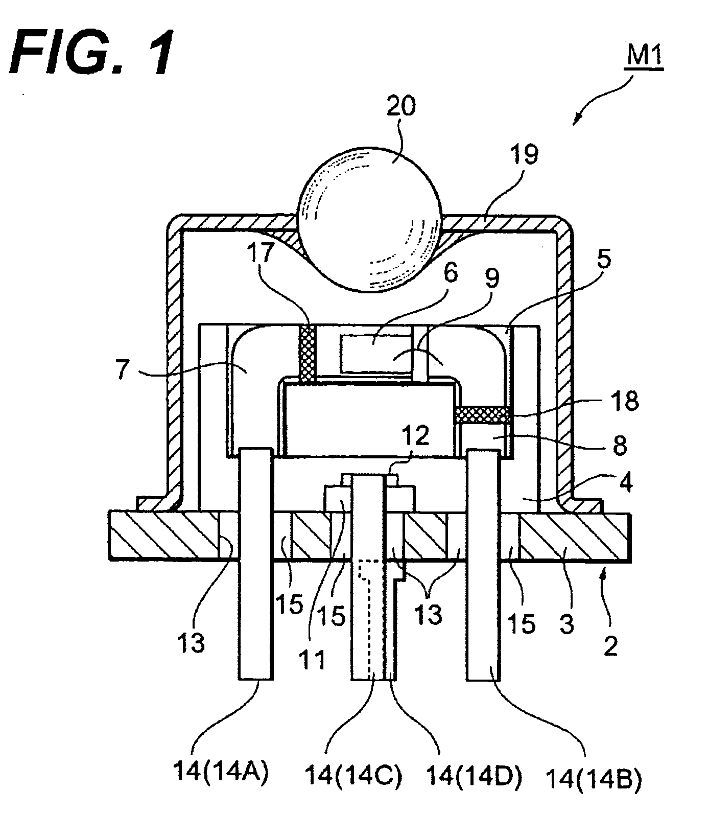
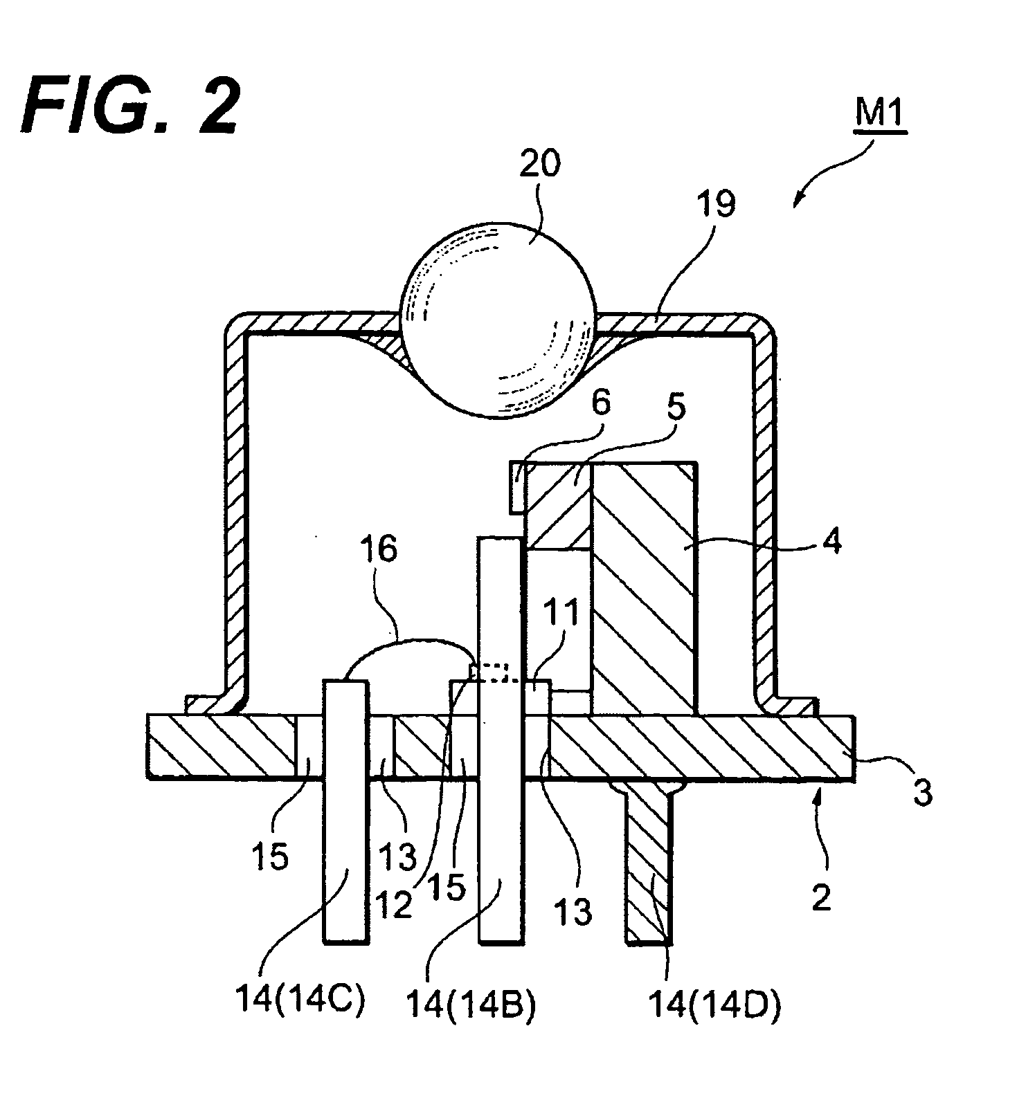
[0026]FIG. 1 is a side cross sectional view, FIG. 2 is a perspective view, and FIG. 3 is a plan cross sectional view of a semiconductor laser module of the first embodiment according to the present invention. As shown in FIGS. 1 to 3, the semiconductor laser module 1 has a stem comprising a disk-shaped base 3 and a block 4 both made of metal, preferably made of copper. The block 4 is placed and fixed on the base 3. In the embodiment shown in FIG. 1, although the block 4 is individually formed from the base 4, it may be integrally formed.

[0027] On the block 4 is provided by a sub-mount 5, for example made of aluminum nitride (AlN), and a semiconductor laser 6 is mounted on the sub-mount 5. The sub-mount 5 shapes a rectangle smaller than the block 4 and mounted on the upper portion of the side surface of the block 4, accordingly, a space is formed beneath the sub-mount 5. Other materials, such as silicon carbide (SiC), boron nitride (BN), diamond, or some ceramics having good thermal...

second embodiment

[0040] Next, the second embodiment of the present invention will be described.

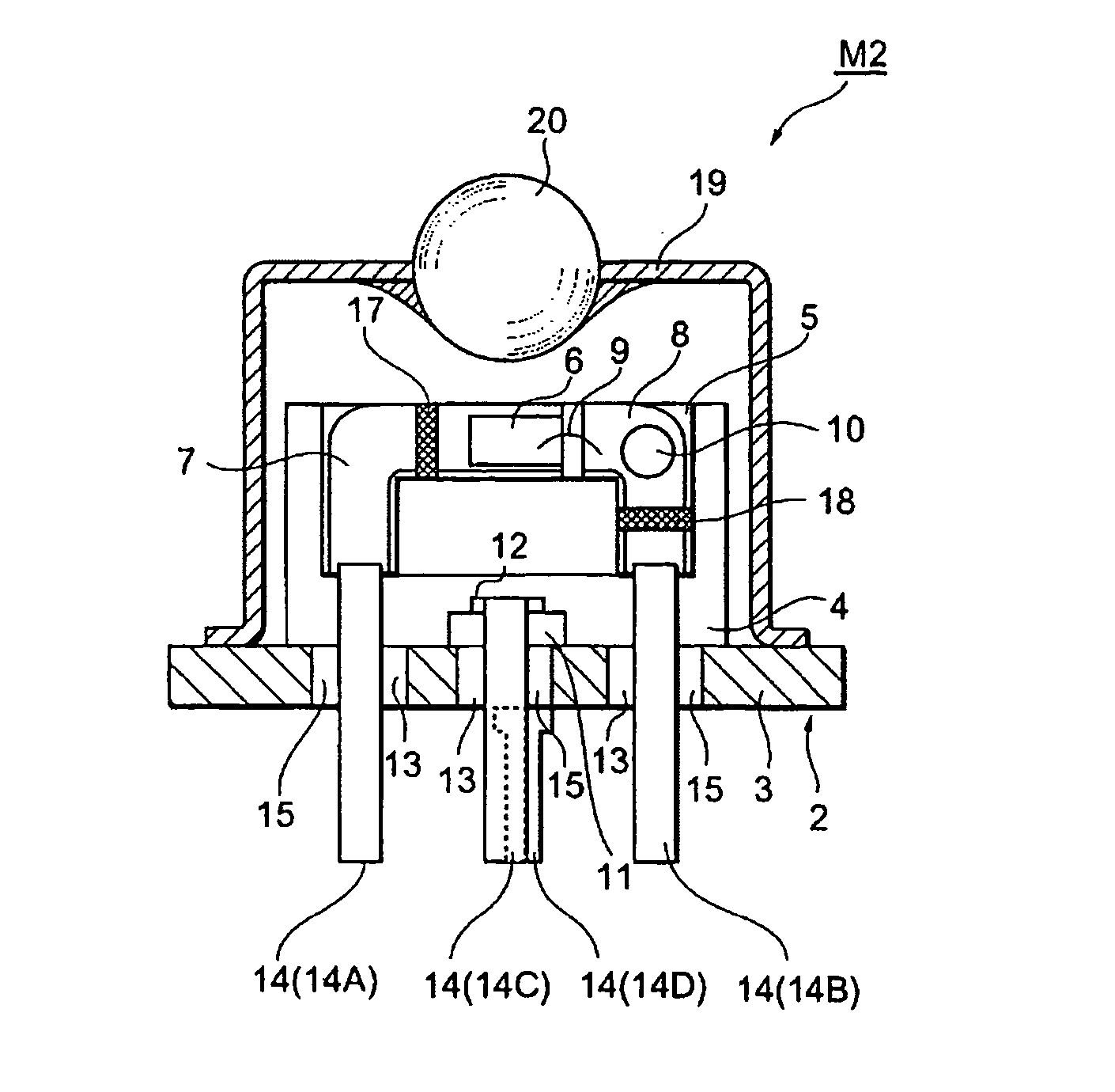
[0041]FIG. 4 is a side cross section view showing the semiconductor laser module M2 according to the second embodiment. The laser module M2 provides, in addition to the laser module M1 of the first embodiment, a via hole 10 in the second transmission line 8 to electrically connect the transmission line 8 to the block 4. The via hole 10 grounds the second transmission line 8 to the block 4. Thus, the anode electrode of the laser diode 6, which is formed on the upper surface thereof, is grounded through the second transmission line 8 and the via hole 10 to the block 4.

[0042] In the laser module M1 of the first embodiment, the normal phase signal and the opposite phase signal can be cancelled at the second transmission line. While in the present laser module M2, both signals can be canceled and grounded at the second transmission line 8. Thus, the EMI noise can be further reduced and the high

third embodiment

[0043]FIG. 5 is a side cross sectional view of the laser module M3 according to the third embodiment. The laser module M3 provides a block 21 having a greater height compared to the block 4 in laser modules previously described.

[0044] The sub-mount 22 for the laser diode in this embodiment provides a first groove 23, a cross section of which has a V-shape, on the upper portion of the side surface thereof. Within in the first groove 23 is disposed by an optical fiber F Another groove 24 with a V-shape relatively larger than the first groove 23, is formed at the region extended from the first groove 23. The latter V-groove 24 is formed deeper than the former V-groove 23, and is disposed a tube therein for protecting the optical fiber F. Further, on the first V-groove 23 is disposed by a cramp 25. Other configurations except for thus described are same as those in the first and second embodiments.

[0045] In the laser module M3, because of the V-groove 23 for disposing the optical fibe...


PUM


Abstract

The present invention provides a semiconductor laser module in which parasitic inductance due to the bonding wire is removed, accordingly, the high frequency performance thereof can be enhanced. The laser module of the present invention has a sub-mount, on which the semiconductor laser diode is installed and transmission lines for supplying the signal to the laser diode is formed. The transmission lines on the sub-mount are directly connected to corresponding lead pins provided in the base of the package without any bonding wires. Between the lead pins and under the sub-mount is provided a photo diode for monitoring light emitted from the laser diode.

Description

BACKGROUND OF THE INVENTION [0001] 1. Field of the Invention [0002] The present invention relates to a semiconductor laser module that provides a co-axial TO-CAN type package and transmission lines therein for complementary driving signal. [0003] 2. Related Prior Art [0004] A conventional laser module having a co-axial shape is shown in FIG. 12. The laser module 60 includes a base 61, a block 62 on the base 61. A sub-mount 63 on which the laser diode 64 is mounted is disposed on the block 62. The base 61 further includes lead pins 65 and 66 electrically isolated from the base 61. One of lead pins 65 is connected to the anode electrode, which is formed on the top surface, of the laser diode 64 via the bonding wire 67. Another lead pin 66 is also connected to the anode electrode of the laser diode and grounded in the outside of the laser module 60. The base further includes the third lead pin 69 connected to the cathode electrode, which is formed on the bottom surface, of the laser di...

Claims


Application Information

Patent Timeline
Patent Type & Authority Applications(United States)
IPC IPC(8): G02B6/36G02B6/42H01S5/022
CPCG02B6/4201H01S5/0683H01S5/02284H01S5/02212H01L2224/48091G02B6/4243G02B6/4245G02B6/4256G02B6/4277G02B6/4279H01S5/02251H01L2924/00014
Inventor KUHARA, YOSHIKIFUNADA, TOMOYUKIFURUMAI, MASAKI
Owner SUMITOMO ELECTRIC IND LTD
Why Eureka
Try Eureka