Stencil mask design method and under bump metallurgy for C4 solder bump

a stencil design and stencil technology, applied in the field of fine-pitch stencil design of printing solder paste and forming under bump metallization pads, can solve the problems of inability to accept technology, high cost and complexity of the stencil printing process, and the inability of most companies to accept technology, so as to eliminate the separation of solder materials, improve the formation of solder balls, and eliminate the effect of bridging

Active Publication Date: 2005-01-20
THE HONG KONG UNIV OF SCI & TECH
View PDF4 Cites 0 Cited by
  • Summary
  • Abstract
  • Description
  • Claims
  • Application Information

AI Technical Summary

Benefits of technology

[0010] According to an embodiment of the present invention, the stencil mask design is dependent on the reflowing enhancement layer 1 and the height of solder bumps. The solder paste is deposited through the printing process on the wafer. During the reflowing process, the solder paste is molten. The solder paste may be shrunken to form a solder ball. The rectangle metal layer 1 can improve the solder ball formation because of the surface tension of the molten solder paste. The solder paste may be shrunken along to the reflowing enhancement layer. The method can eliminate the separation of solder material during the reflowing process. And it also eliminates the bridging and reduces the space between the solder balls.

Problems solved by technology

The solder bumping process that IBM invented is expensive and complicated because the solder material is deposited by an evaporation process through a metal mask.
Most companies cannot accept the technology due to the cost.
Although the plating bumping process is cheaper than the metal evaporation process, the facility system is more expensive than a stencil printing process.
However, the conventional stencil printing process cannot provide the small pitch solder bumps.
The fine-pitch solder bumps cannot be prepared by the conventional stencil printing process.

Method used


Image

  • Stencil mask design method and under bump metallurgy for C4 solder bump
  • Stencil mask design method and under bump metallurgy for C4 solder bump
  • Stencil mask design method and under bump metallurgy for C4 solder bump

Examples


Embodiment Construction

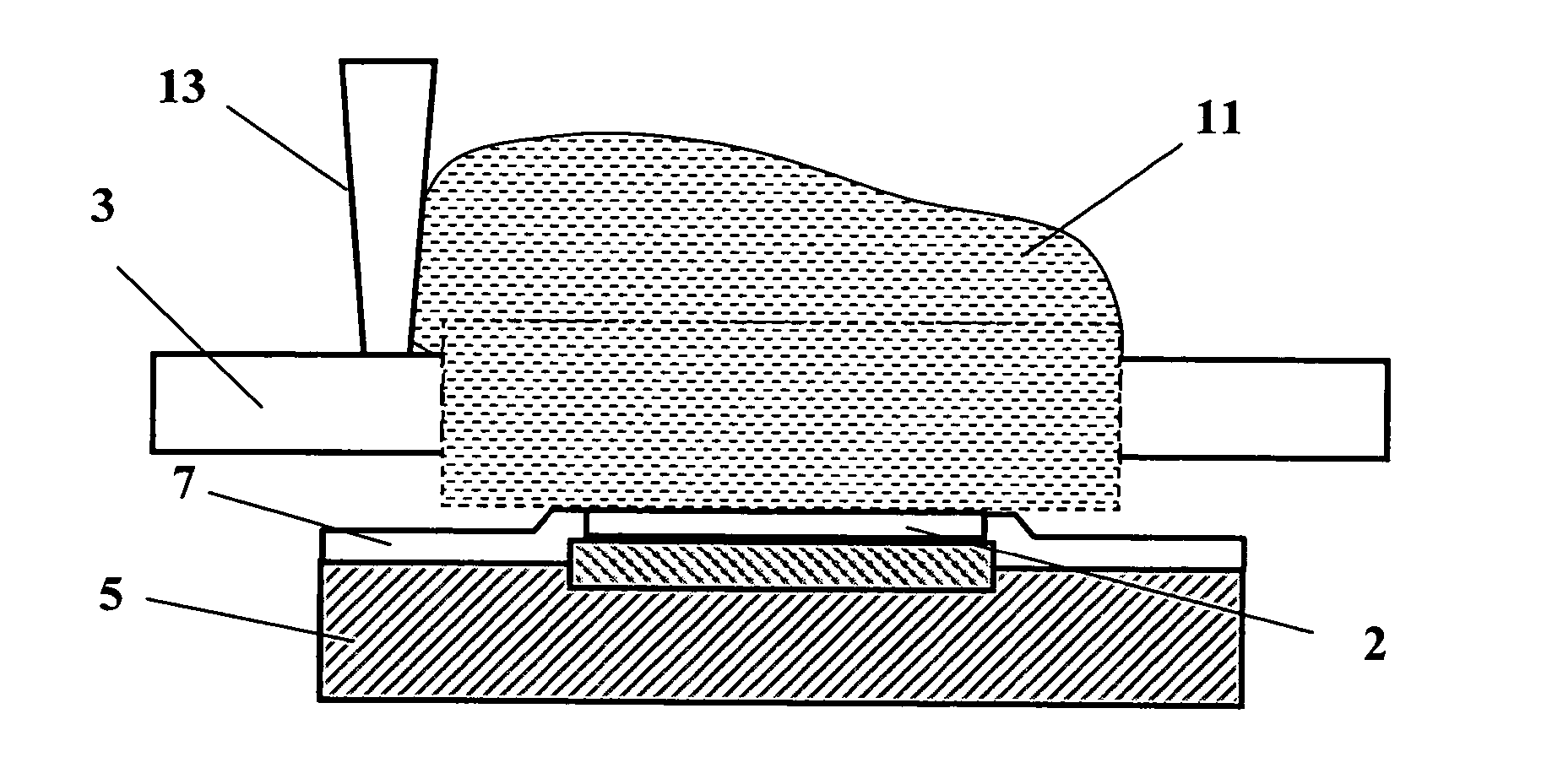
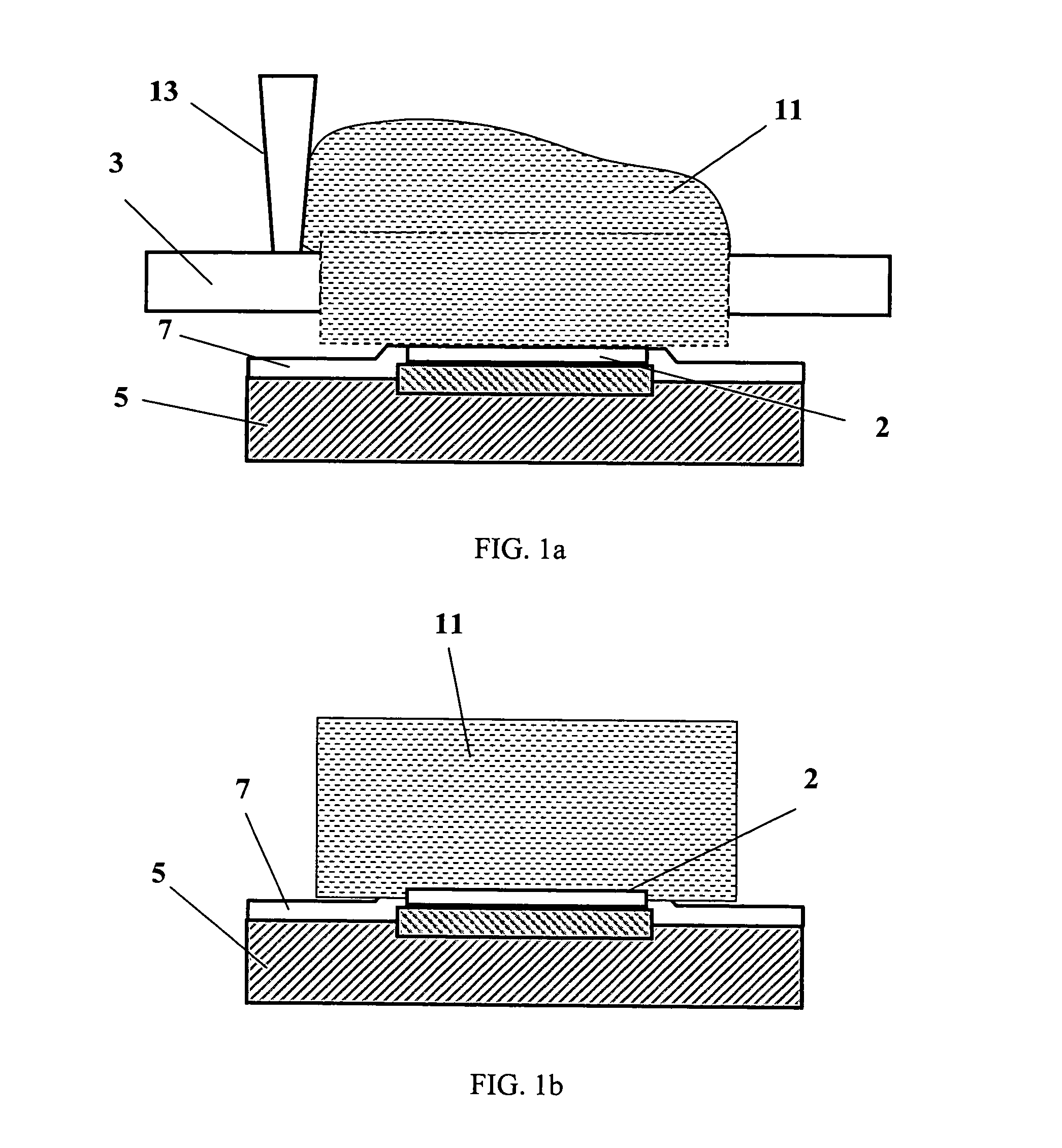
[0017] According to the present invention, an embodiment is described using some relevant materials. The detailed processes, method and designs are illustrated according to the drawings.

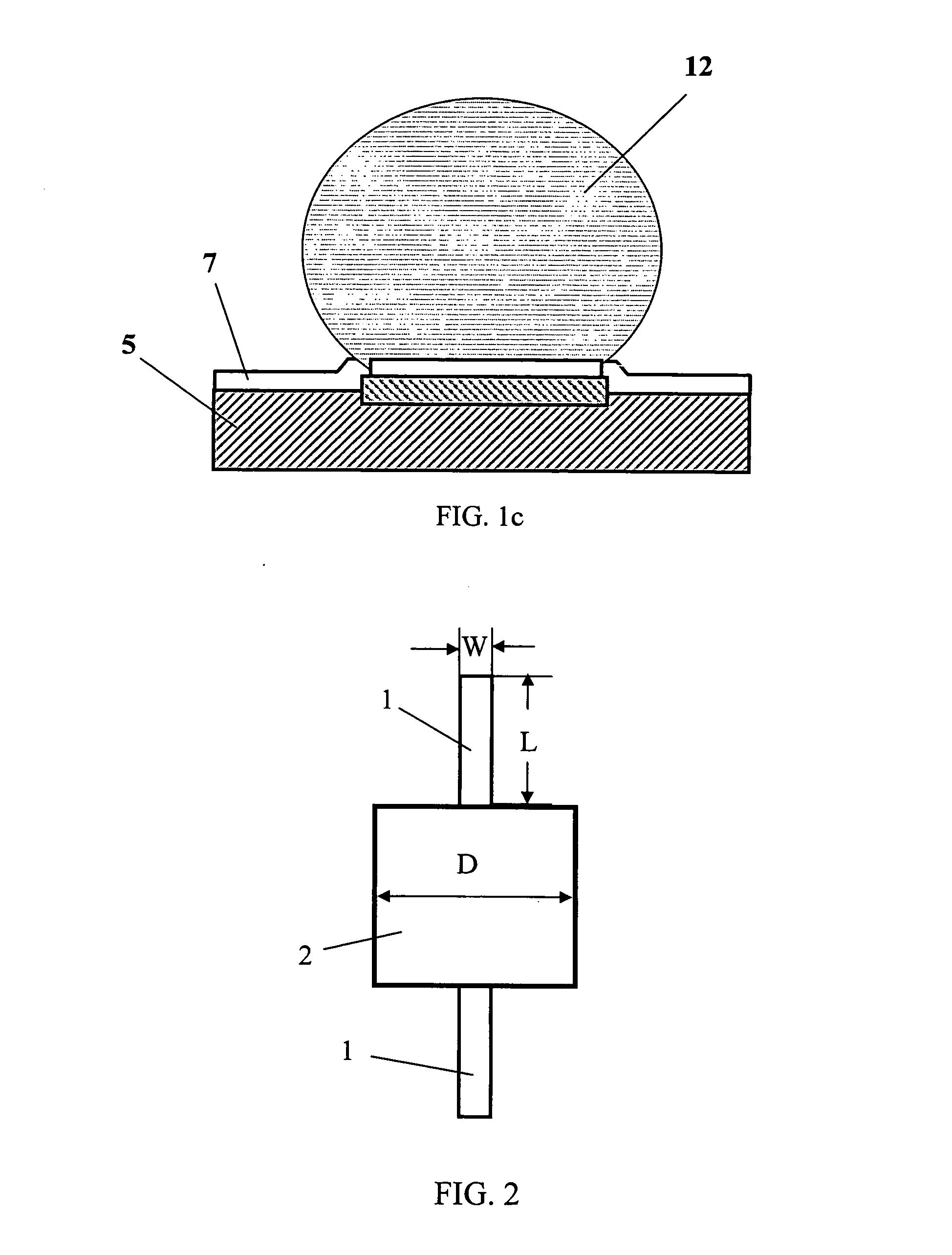
[0018]FIGS. 3a-3b illustrate the design method of stencil mask 3. The opening pattern 4 of stencil mask 3 needs to match the UBM layer 2 and the reflowing enhancement layer 1. The opening size of pattern 4 on the stencil mask 3 defines the height of solder bumps 12. An average length of the opening pattern 4 on the stencil mask 3 is defined as half of the sum of length L2 and width W2. In order to eliminate the solder paste 11 sticking up the solder mask 3, a ratio of the average length ((L2+W2) / 2) of the opening pattern 4 on the stencil mask 3 to the thickness T of the stencil mask 3 is from 2.4 to 3. And the opening length L2 of the opening pattern 4 on the stencil mask 3 is a little longer than the total length (D+2L) of the UBM layer 2 and the reflowing enhancement layer 1 as shown in FIG. 3b.

[...


PUM

PropertyMeasurementUnit
volume ratioaaaaaaaaaa

Abstract

A method for the fine-pitch stencil mask design for stencil printing bumping technology for eutectic Sn / Pb and lead-free solder material is described. In the method, a reflowing enhancement layer is introduced to improve the solder quality and reduce the pitch of solder bumps. The method of forming the layer is described as well as the forming method of matching under-bump metallurgy layer. The method of stencil mask design can match various sizes and pitch of the solder bumps. The designed mask is fixed on the stencil printer to deposit the solder materials with the required patterns. This method can increase the solder paste volume to increase the height of solder bumps after the reflowing process.

Description

CROSS-REFERENCE TO RELATED APPLICATIONS [0001] The present invention claims priority of CN 03142416.3, filed on Jun. 3, 2003, the entire contents of which is incorporated herein by reference. FIELD OF THE INVENTION [0002] The present invention relates to electronic packaging, and more particularly to a fine-pitch stencil mask design method of printing solder paste and forming under bump metallization pads on a semiconductor substrate for flip chip attachment. BACKGROUND OF THE INVENTION [0003] In the early 1960s, the flip chip technology and controlled-collapse-chip connection (C4) technology were introduced by IBM to interconnect ICs to their substrates. A flip chip is a chip that is flipped face down and bonded to the substrate with various interconnection materials and methods such as tape-automated bonding, solder bumps, wire interconnects, isotropic and anisotropic conductive adhesives, and so on. The flip-chip solder preparation process generally composes of UBM (Under Bump Me...

Claims


Application Information

Patent Timeline
Patent Type & Authority Applications(United States)
IPC IPC(8): H01L21/28H01L21/44H01L21/60H01L21/768H01L23/485
CPCH01L24/11H01L2224/13099H01L2924/0001H01L2224/131H01L2924/014H01L2924/01022H01L2924/01029H01L2924/01033H01L2924/01047H01L2924/01074H01L2924/01078H01L2924/01079H01L2924/01082H01L2924/01322H01L2924/14H01L24/13H01L2924/01005H01L2924/01006H01L2924/01023H01L2924/01024H01L24/03H01L24/05H01L2224/05001H01L2224/05022H01L2224/05571H01L2224/05644H01L2924/00014H01L2224/05099
Inventor CHAN, CHINGHO PHILIPXIAO, GUOWEI DAVID
Owner THE HONG KONG UNIV OF SCI & TECH
Why Eureka
Try Eureka