Insulated gate bipolar transistor with built-in freewheeling diode

a bipolar transistor and freewheeling diode technology, applied in the field of bipolar transistors, can solve the problems of significant degradation of igbt, low conductivity of power moseft, and unsuitability of power moseft for high current applications

Inactive Publication Date: 2005-01-27
MITSUBISHI ELECTRIC CORP
View PDF21 Cites 120 Cited by
  • Summary
  • Abstract
  • Description
  • Claims
  • Application Information

AI Technical Summary

Benefits of technology

[0022] The present invention produces an advantage of maintaining both electrical characteristics (VCE(sat)) exhibited when the insulated gate bipolar transistor with the built-in freewheeling diode serves as an IGBT and electrical characteristics (Vf) exhibited when the insulated gate bipolar transistor with the built-in freewheeling diode serves as a diode, at a relatively low level suitable for practical use.
[0023] More specifically, the second semiconductor layer occupies 30-80% of the second main surface in footprint, so that VCE(sat) of the

Problems solved by technology

Thus, when the IGBT performs a switching operation to suddenly interrupt the current flowing through the motor, the characteristics of the IGBT is significantly degraded because of the released energy.
However, a density of a conductible current of the power MOSEFT is relatively low, and thus the power MOSEFT is unsuitable for high current applications.
Such voltage is too high as a breakdown voltage of a freewheeling diode.
Because of presence of a barrier having such a high breakdown voltage, characteristics of the IGBT may be significantly degraded upon generation of heat due to a voltage applied during freewheeling.
However, it should be noted that both JP 7-153942 a

Method used


Image

  • Insulated gate bipolar transistor with built-in freewheeling diode
  • Insulated gate bipolar transistor with built-in freewheeling diode
  • Insulated gate bipolar transistor with built-in freewheeling diode

Examples


first preferred embodiment

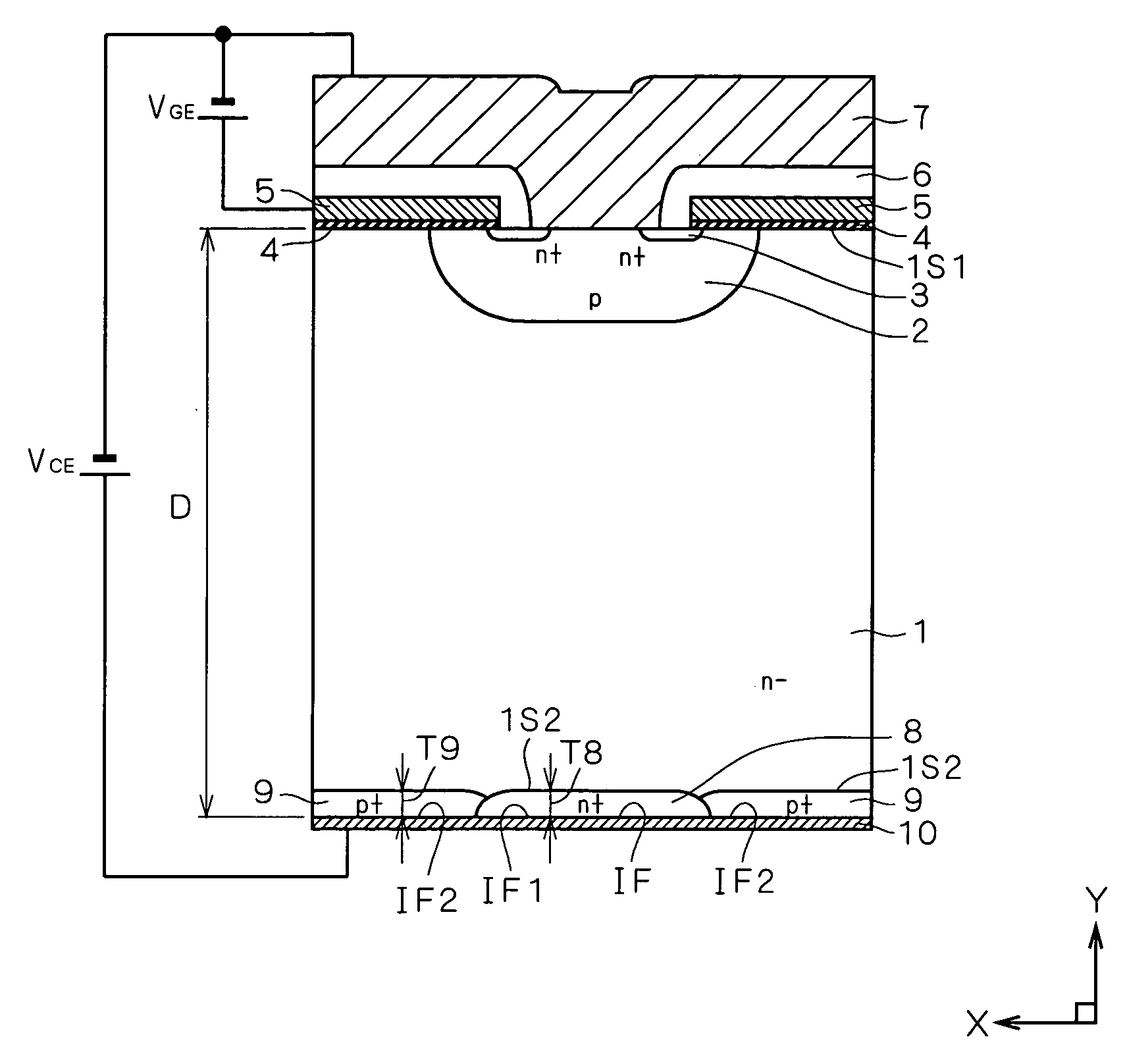
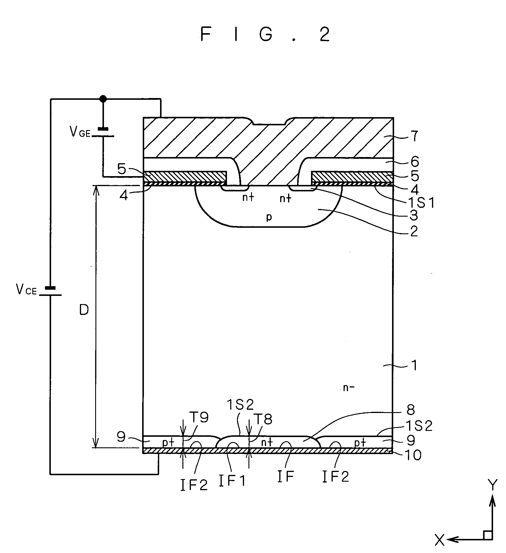
[0041]FIG. 2 is a longitudinal sectional view of a portion of an exemplary structure of an IGBT with a built-in freewheeling diode (semiconductor device) according to a first preferred embodiment. In FIG. 2, a direction “X” is a width direction along a width of a silicon wafer, and a direction “Y” is a thickness direction along a thickness of the silicon wafer. The semiconductor device illustrated in FIG. 2 is achieved by applying the following features of the first preferred embodiment to an IGBT with a built-in freewheeling diode including a MOSFET cell having a DMOS structure.

[0042] First, the silicon wafer of the semiconductor device in FIG. 2 includes: 1) as a core portion of the silicon wafer, an N−-type semiconductor substrate (which will be also referred to as an “N−-type layer”) 1 containing an impurity of a first conductivity type (N type in the present example), which includes a first main surface 1S1 and a second main surface 1S2; and 2) a cell of an insulated gate tran...

second preferred embodiment

[0066]FIG. 13 is a longitudinal sectional view of an IGBT with a built-in FWD according to a second preferred embodiment. A device illustrated in FIG. 13 is formed by additionally providing an N-type layer 11 in the device illustrated in FIG. 12 which includes a trench MOSFET cell with a gate electrode buried in each trench formed inside the N−-type layer 1. The N-type layer 11 is horizontally interposed between adjacent trenches and is vertically interposed between the P-type base region 2 and the N−-type layer 1. The device illustrated in FIG. 13 is identical in structure to the device illustrated in FIG. 12 in the other respects.

[0067] Operations of the device illustrated in FIG. 13, when it serves as the IGBT, are basically identical to those illustrated in FIG. 12. However, in the device illustrated in FIG. 13, the N-type layer 11 having a higher impurity concentration than that of the N−-type semiconductor substrate 1 is additionally provided immediately under the P-type base...

third preferred embodiment

[0075] A method of manufacturing an IGBT with a built-in FWD according to a third preferred embodiment essentially includes: 1) forming an MOSFET cell and a first main electrode used for the IGBT in a region on a first main surface side of a semiconductor substrate of a first conductivity type; 2) polishing the semiconductor substrate provided after formation of the MOSFET cell, from a second main surface thereof (a surface opposite and substantially parallel to the first main surface), to make a thickness of the semiconductor substrate equal to 200 μm or smaller; 3) forming a first semiconductor layer of the first conductivity type and a second semiconductor layer of a second conductivity type adjacent to the first semiconductor layer such that the first and second semiconductor layers extend from a region of the second main surface of the polished semiconductor substrate which faces the MOSFET cell toward an interior of the semiconductor substrate; and 4) forming a second main ele...


PUM


Abstract

In an IGBT with a built-in freewheeling diode, a thickness (D) of a polished wafer is equal to 200 μm or smaller, and each of respective thicknesses (T8) and (T9) of an N+-type cathode layer (8) and a P+-type collector layer (9) is equal to 2 μm or smaller. Further, a total width of the N+-type cathode layer (8) and the P+-type collector layer (9) which extends along a width direction (X) is in a range from 50 μm to 200 μm. In this case, an interface (IF2) between a collector electrode (10) and the P+-type collector layer (9) occupies 30-80% of an interface (IF) between the collector electrode (10) and the P+-type collector layer (9) plus the N+-type cathode layer (8).

Description

BACKGROUND OF THE INVENTION [0001] 1. Field of the Invention [0002] The present invention relates to a bipolar transistor including an insulated gate (MOS structure), and more particularly to a structure of an insulated gate bipolar transistor (which will hereinafter be abbreviated as an “IGBT”, and may be also referred to as a “reverse conducting IGBT” in general) including a built-in freewheeling diode (which will hereinafter be also abbreviated as a “FWD”), and a technique for manufacturing the same. The IGBT according to the present invention can be used as a switching device with a built-in FWD in an inverter circuit for driving a load such as a motor, for industrial purposes. [0003] 2. Description of the Background Art [0004] In power electronics for driving a motor or the like, under a condition that a rated voltage is 300V or higher, an IGBT is usually used as a switching device because of its characteristics. In using an IGBT as a switching device, a freewheeling diode (FWD...

Claims


Application Information

Patent Timeline
IPC IPC(8): H01L21/331H01L21/336H01L27/04H01L29/06H01L29/08H01L29/739H01L29/76H01L29/78
CPCH01L29/0696H01L29/7395H01L29/66333H01L29/0834H01L21/02233H01L29/1095H01L29/66325H01L29/7393H01L29/7397H01L29/7813H01L2924/13055
Inventor TAKAHASHI, HIDEKIAONO, SHINJI
Owner MITSUBISHI ELECTRIC CORP
Why Eureka
Try Eureka