

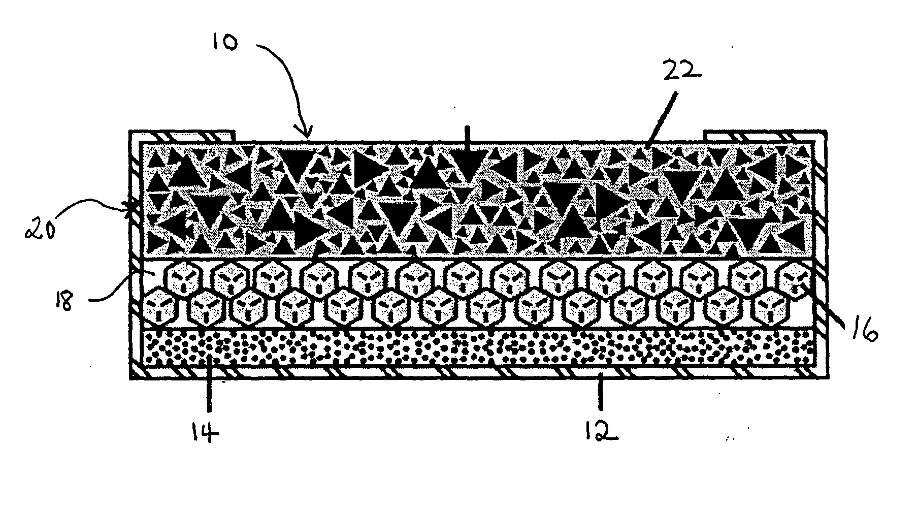
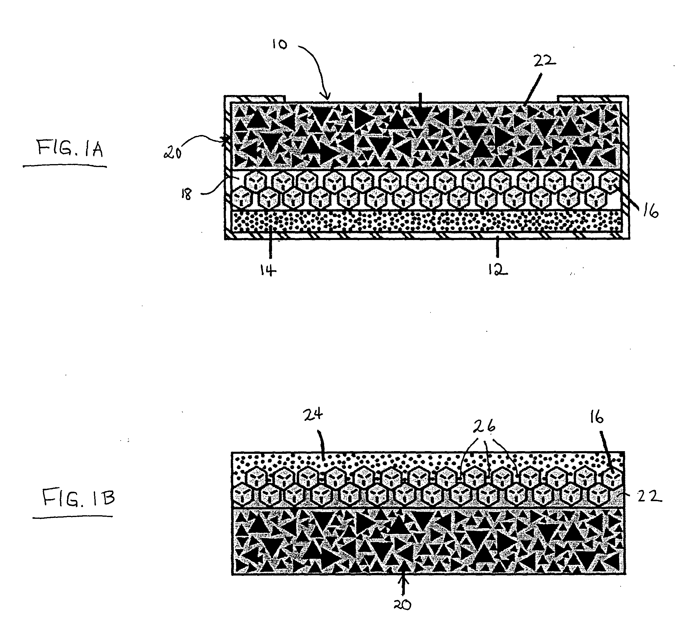
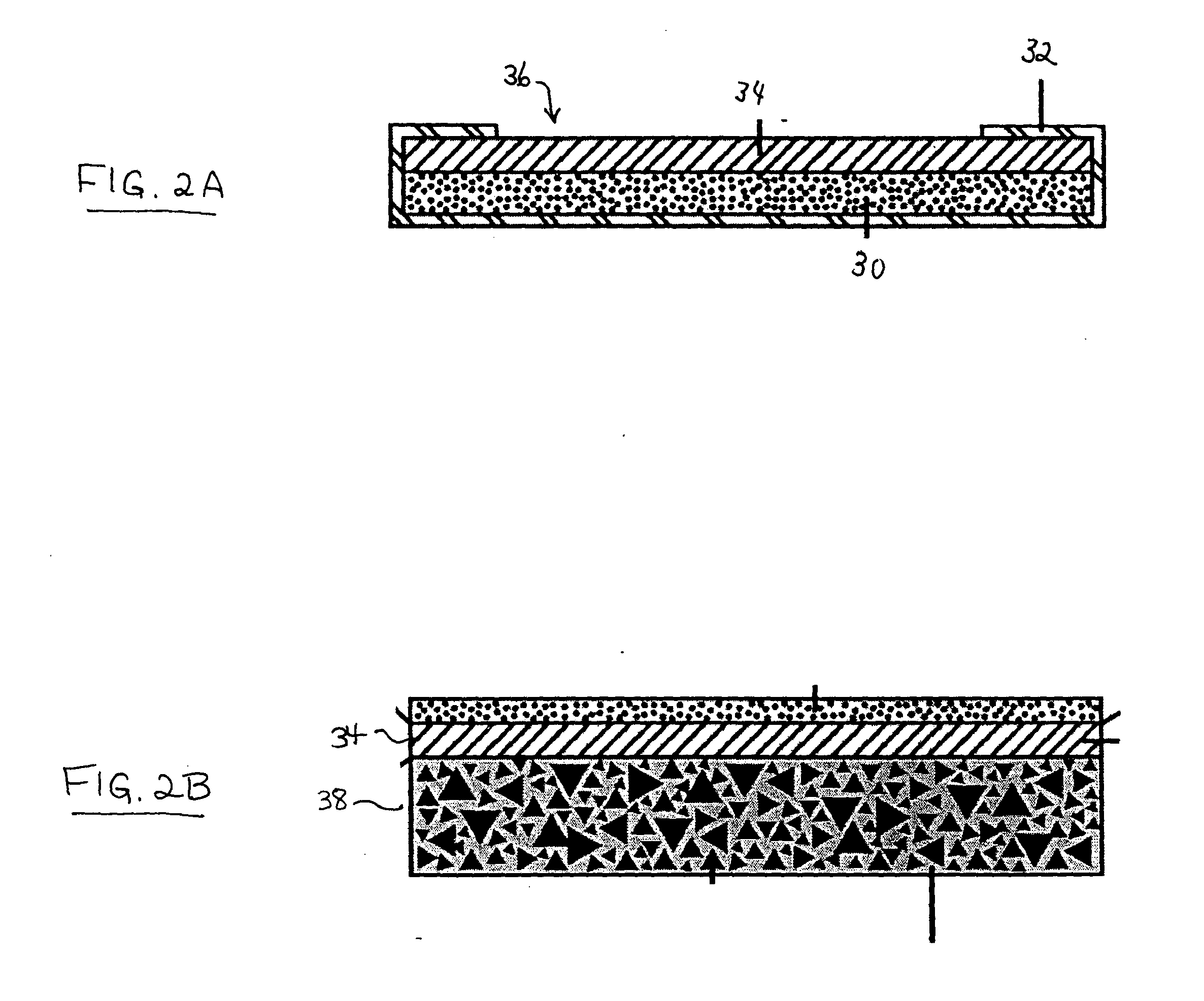
Nanodiamond PCD and methods of forming
a technology of diamond pcd and diamond, applied in the field of diamond tools, can solve the problems of increasing production costs and manufacturing complexity, lack of requisite strength for most mechanical applications, etc., and achieve the effect of improving high temperature performan
- Summary
- Abstract
- Description
- Claims
- Application Information
AI Technical Summary
Benefits of technology
Problems solved by technology
Method used
Image

Examples
example 1
[0051] A layer of nanodiamond having an average particle size of about 5 nm is placed in a tantalum cup to a thickness of about 2 mm. A layer of 40 / 50 mesh diamond is then placed over the nanodiamond layer to a thickness of 1 mm. A cobalt cemented tungsten carbide substrate measuring about 10 mm in thickness was then placed against the 40 / 50 mesh diamond layer to form a tool precursor. The assembled tool precursor is then placed in a HTHP apparatus and pressed to about 4 GPa and heated to about 1,800° C. for about 40 minutes. The cobalt infiltrates through the 40 / 50 mesh diamond layer, but not into the nanodiamond layer. The nanodiamond layer is sintered. The sintered mass is then allowed to cool and removed from the apparatus.
example 2
[0052] A layer of nanodiamond having an average particle size of about 5 nm is placed in a tantalum cup to a thickness of about 5 mm. A tungsten substrate measuring about 10 mm in thickness was then placed against the nanodiamond layer to form a tool precursor. The assembled tool precursor is then placed in a HTHP apparatus and pressed to about 4 GPa and heated to about 1,600° C. for about 60 minutes. The nanodiamond layer is sintered and then allowed to cool. The sintered product is then removed from the apparatus and brazed to a tungsten carbide substrate using a silver braze.
example 3
[0053] A mixture of 10% by weight cobalt, 5% by weight organic binder, and 85% by weight tungsten carbide is placed in an annular shape along the inside of a tantalum cup to a thickness of 5 mm. A layer of 40 / 50 mesh diamond in an organic binder is then layered over the tungsten layer to a thickness of 1 mm. The remaining space is filled with nanodiamond having an average particle size of 100 μm. The assembled tool precursor is then preheated to about 800° C. to remove the organic binder and then placed in a HTHP apparatus and pressed to about 5 GPa and heated to about 2,000° C. for about 45 minutes. The cobalt infiltrates through the 40 / 50 mesh diamond layer, but not into the nanodiamond layer. The nanodiamond layer is sintered. The sintered mass is then allowed to cool and removed from the apparatus. An aperture is then cut into the nanodiamond section having a profile similar to that shown in FIG. 3B to form a wire drawing die.
PUM
| Property | Measurement | Unit |
|---|---|---|
| diameter | aaaaa | aaaaa |
| diameter | aaaaa | aaaaa |
| diameter | aaaaa | aaaaa |
Abstract
Description
Claims
Application Information