Semiconductor device with floating trap type nonvolatile memory cell and method for manufacturing the same

US20050023604A1Active Publication Date: 2005-02-03SAMSUNG ELECTRONICS CO LTD

Image

  • Semiconductor device with floating trap type nonvolatile memory cell and method for manufacturing the same
  • Semiconductor device with floating trap type nonvolatile memory cell and method for manufacturing the same
  • Semiconductor device with floating trap type nonvolatile memory cell and method for manufacturing the same

Examples


Embodiment Construction

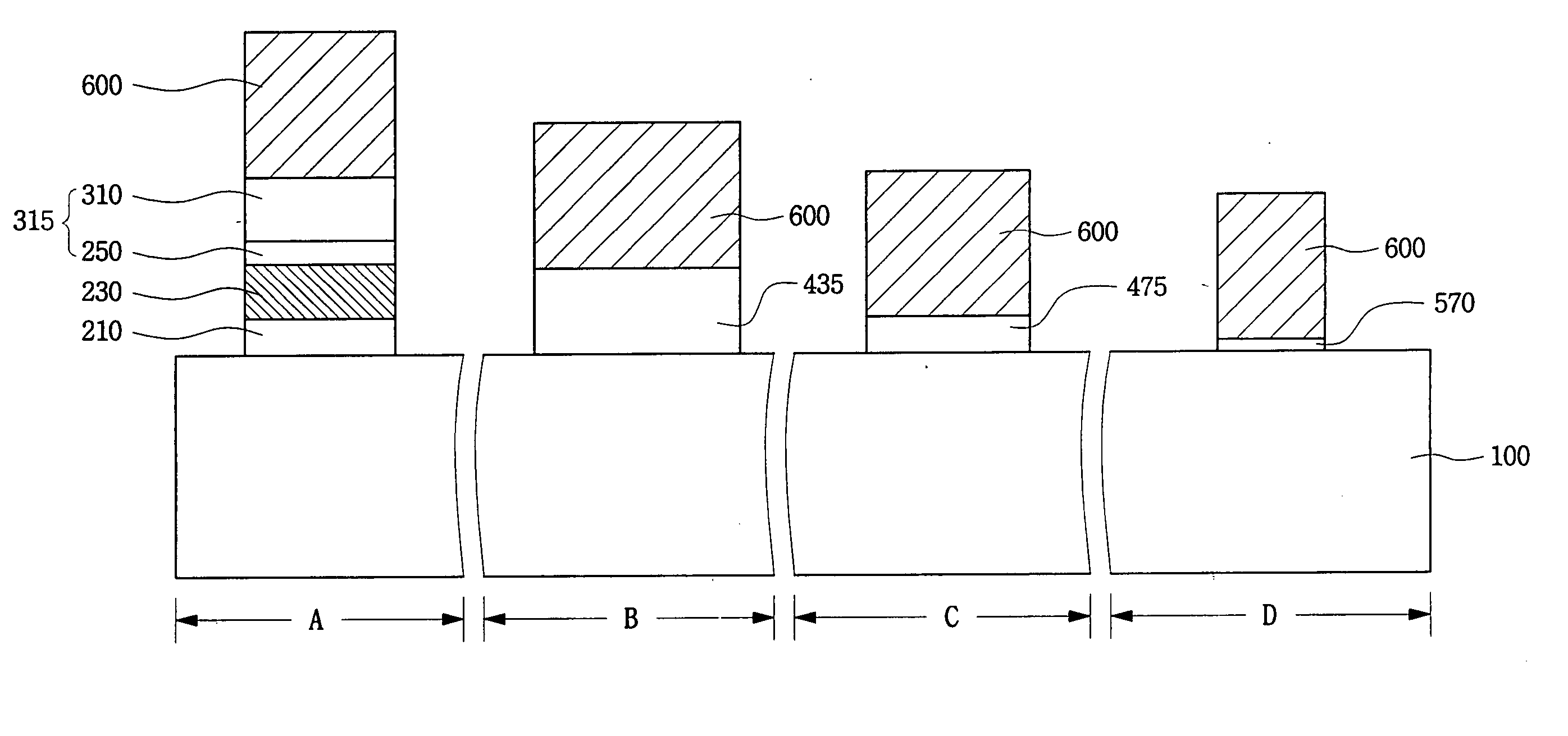
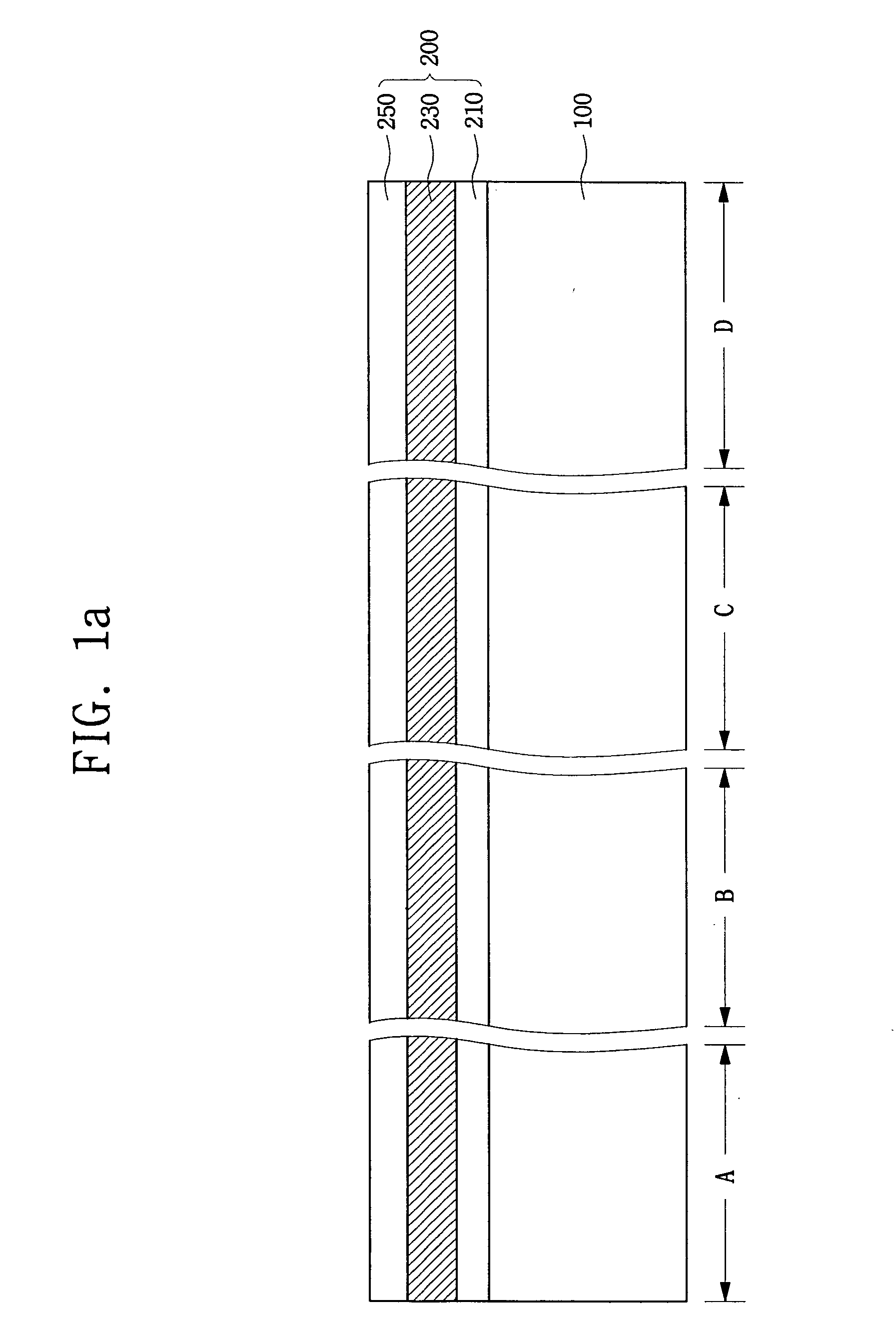
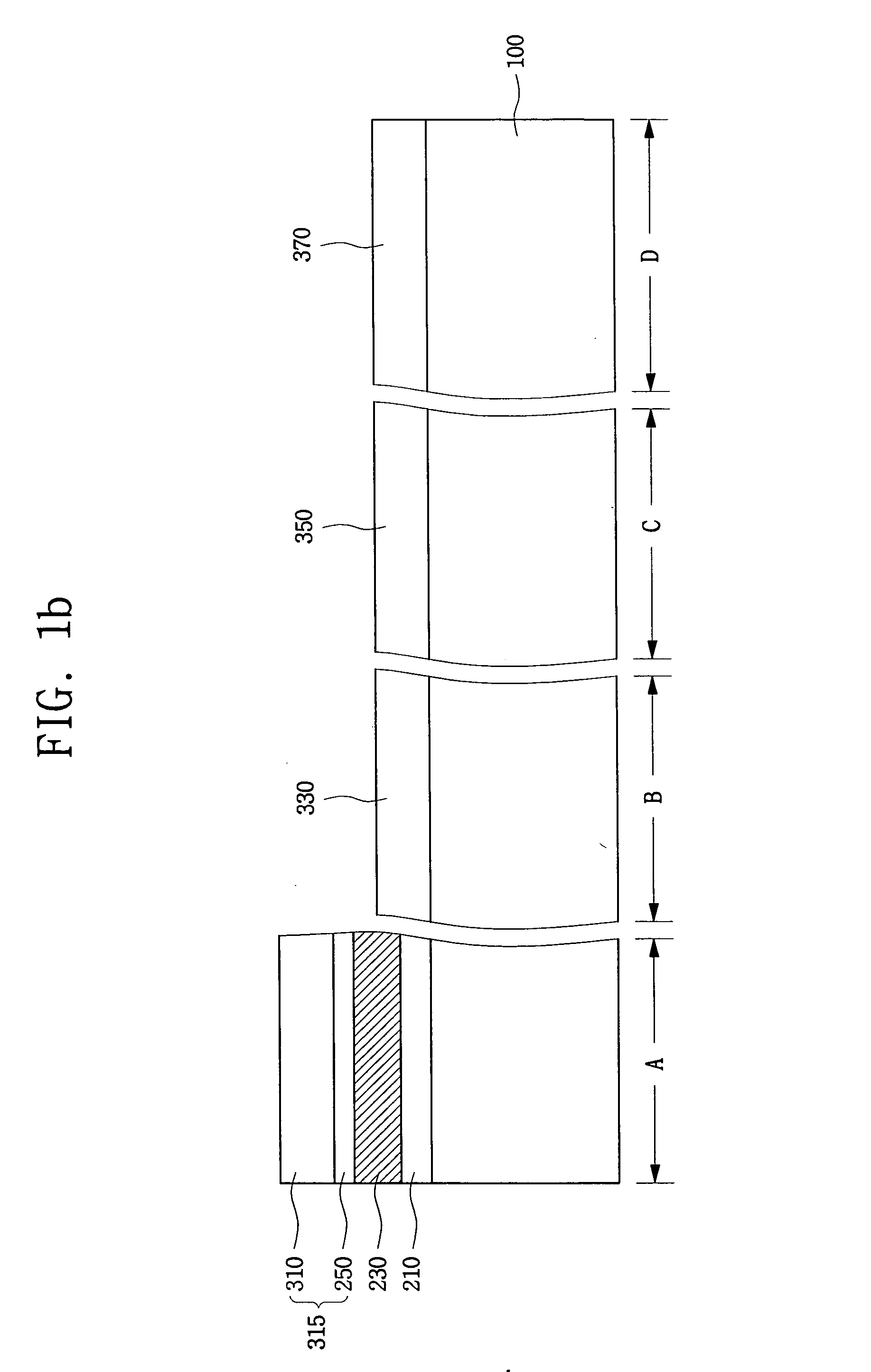
[0023] The present invention will now be described more fully hereinafter with reference to the accompanying drawings, in which preferred embodiments of the invention are shown. In the drawings, the thickness of layers and regions are exaggerated for clarity. FIG. 1a to FIG. 1e are cross-sectional views illustrating a method for manufacturing a semiconductor device having a floating trap type nonvolatile memory cell in accordance with one embodiment of the present invention.

[0024] Referring to FIG. 1a, a semiconductor substrate 100 comprising a nonvolatile memory region A, a first region B, and a second region C is provided. The semiconductor substrate 100 may further comprise a third region D. Each of the first region B, the second region C, and the third region D has a different voltage applied. More specifically, the first region B and the third region D have a high voltage and low voltage, respectively, applied. The second region C has applied a medium voltage between the high ...


PUM


Abstract

The present invention discloses a semiconductor device having a floating trap type nonvolatile memory cell and a method for manufacturing the same. The method includes providing a semiconductor substrate having a nonvolatile memory region, a first region, and a second region. A triple layer composed of a tunnel oxide layer, a charge storing layer and a first deposited oxide layer on the semiconductor substrate is formed sequentially. The triple layer on the semiconductor substrate except the nonvolatile memory region is then removed. A second deposited oxide layer is formed on an entire surface of the semiconductor substrate including the first and second regions from which the triple layer is removed. The second deposited oxide layer on the second region is removed, and a first thermal oxide layer is formed on the entire surface of the semiconductor substrate including the second region from which the second deposited oxide layer is removed. The semiconductor device can be manufactured according to the present invention to have a reduced processing time and a reduced change of impurity doping profile. The thickness of a blocking oxide layer and a high voltage gate oxide layer can be controlled.

Description

CROSS-REFERENCE TO RELATED APPLICATION [0001] This application claims the benefit of Korean Patent Application No. 2003-52896, filed on Jul. 30, 2003, the contents of which are hereby incorporated herein by reference in their entirety.BACKGROUND OF THE INVENTION [0002] 1. Field of the Invention [0003] The present invention relates to a semiconductor device and a method for manufacturing the same and, more particularly, to a semiconductor device having a floating trap type nonvolatile memory cell and a method for manufacturing the same. [0004] 2. Description of the Related Art [0005] A nonvolatile memory such as a flash memory can maintain data until a removal operation is performed after the data are input. Therefore, the nonvolatile memory does not require a refresh operation so that power consumption can be reduced compared to a volatile memory such as a Dynamic Random Access Memory (DRAM). [0006] However, a high voltage is typically required to be applied to the nonvolatile memor...

Claims


Application Information

Patent Timeline
03 Feb 2005
Publication
US20050023604A1
IPC
H01L21/8234; H01L21/8246; H01L21/8247; H01L27/105; H01L27/115
CPC
H01L21/823462; H01L27/105; H01L27/11568; H01L27/11526; H01L27/11546; H01L27/115; H10B41/49; H10B41/40
Inventors
KIM, SANG-SU; KOH, KWANG-WOOK