Driving apparatus of a light-emitting device

a technology of light-emitting devices and driving apparatuses, which is applied in the direction of dc level restoring means or bias distort correction, pulse techniques, and baseband system details, etc., can solve the problems of delay in the light output of the laser diode, the control of the driving current flowing through the laser diode becomes unstable, and the optical noise increases. , to achieve the effect of stable control, control of operation and high accuracy

Inactive Publication Date: 2005-02-03
LAPIS SEMICON CO LTD
View PDF3 Cites 17 Cited by
  • Summary
  • Abstract
  • Description
  • Claims
  • Application Information

AI Technical Summary

Benefits of technology

[0017] When the offset voltage exists in a differential output section, there is concern that the offset voltage component is included in a positive phase voltage signal and a negative phase voltage signal output from the differential output section. In this connection, the driving apparatus of the present invention processes the positive phase voltage signal and the negative phase voltage signal in the first calculation section so as to remove the offset voltage component. Based on the calculation result in the first calculation section, a level of a first DC current is adjusted. Accordingly, an operation of the light-emitting device is stably controlled without being influenc

Problems solved by technology

When an offset voltage of the operational amplifier included in a driving control circuit for the laser diode increases, the control of the driving current flowing through the laser diode becomes unstable, because an optical amplitude value or an optical peak value can not be accurately detected.
When a driving bias current far exceeds a light-emitting threshold value, a light-emitting state remains during an off period of the light output from the laser diode, and thus an optical noise increases during the off period.
On the other hand, when the driving bias current decreases, a transient response time from an optical turning off to a

Method used


Image

  • Driving apparatus of a light-emitting device
  • Driving apparatus of a light-emitting device
  • Driving apparatus of a light-emitting device

Examples


first embodiment

[0058] First Embodiment of Driving Apparatus

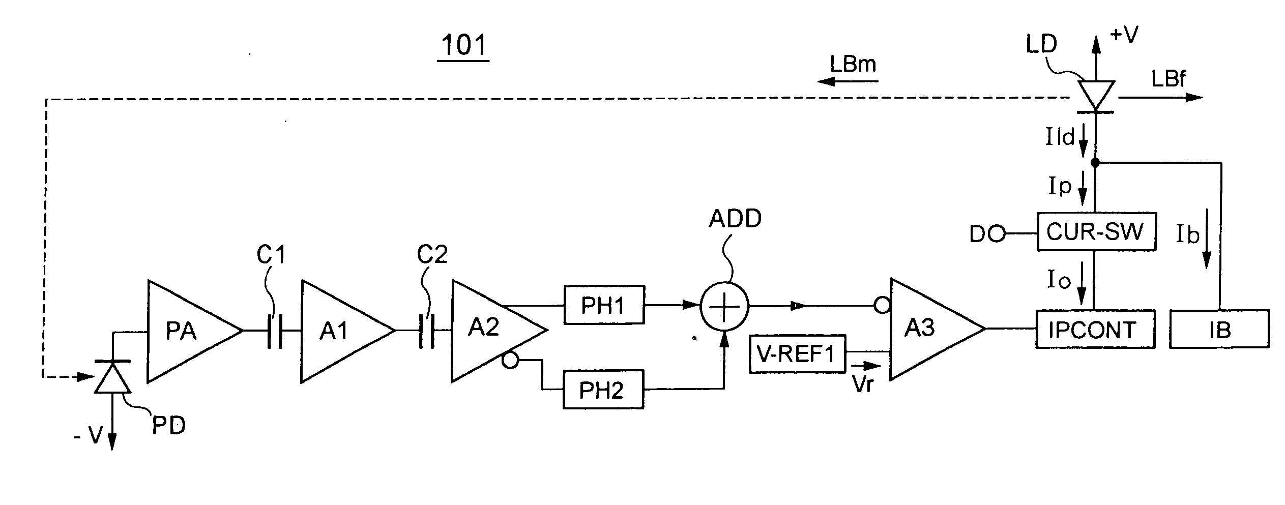
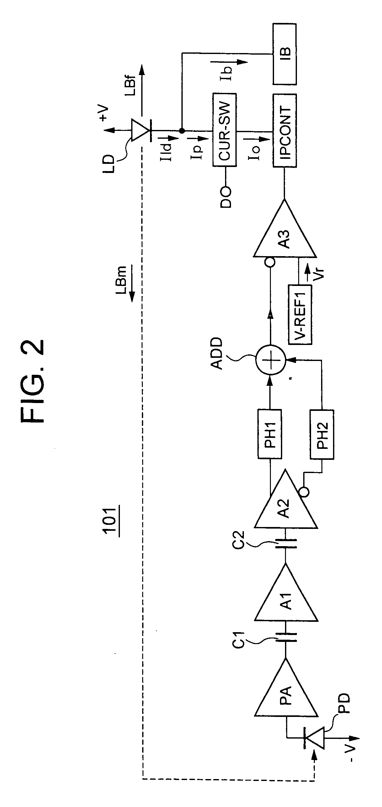
[0059] A laser diode driving circuit (a driving apparatus of a light-emitting device) 101 according to a first embodiment of the present invention is shown in FIG. 2.

[0060] The laser diode driving circuit 101 includes a laser diode LD (light-emitting device), a photodiode PD (light-receiving device), a preamplifier section PA (current-to-voltage converting section), a capacitor C1, an AC (Alternating Current) signal amplifier A1, a capacitor C2, a differential output amplifier A2 (differential output section), a first peak hold circuit PH1 (first detector circuit), a second peak hold circuit PH2 (second detector circuit), an adding circuit ADD, a reference voltage circuit V-REF1 (first reference voltage circuit), a differential input amplifier A3, a current output circuit IPCONT (first DC current output section), a current switch circuit CUR-SW (pulse current output section), and a bias current circuit IB (bias current output section). Th...

second embodiment

[0126] Second Embodiment

[0127] A laser diode driving circuit (a driving apparatus of a light-emitting device) 201 according to a second embodiment of the present invention is shown in FIG. 10.

[0128] As compared with the laser diode driving circuit 101 of the first embodiment shown in FIG. 2, the laser diode driving circuit 201 has such a configuration that a bias current circuit IBCONT is provided in place of the bias current circuit IB and a second differential input amplifier A5 and a second reference voltage circuit V-REF2 are added. The second differential input amplifier A5 forms a second calculation section of the present invention.

[0129] The second differential input amplifier A5 amplifies and outputs a voltage difference between a second reference voltage Vr2 output from the second reference voltage circuit V-REF2 and an output signal of the first peak hold circuit PH1.

[0130] The bias current circuit IBCONT outputs a DC bias current Ib based on an output voltage from the ...

third embodiment

[0150] Third Embodiment

[0151] A laser diode driving circuit (a driving apparatus of a light-emitting device) 301 according to a third embodiment of the present invention is shown in FIG. 13.

[0152] As compared with the laser diode driving circuit 201 of the second embodiment shown in FIG. 10, the laser diode driving circuit 301 has such a configuration that a differential input-output amplifier A2-2 is provided in place of the differential output amplifier A2 and a third reference voltage circuit V-REF3 is added.

[0153] A third reference voltage Vr3 output from the third reference voltage circuit V-REF3 is adjusted so as to coincide with an electrical potential of a voltage signal output from the preamplifier section PA on the condition that no input is supplied to the preamplifier section PA. The temperature fluctuation or the power supply fluctuation are included in the above condition. The third reference voltage circuit V-REF3 may be configured by using, for example, a circuit s...


PUM


Abstract

A first peak hold circuit holds a peak potential of a positive phase voltage signal output from a differential output amplifier, and a second peak hold circuit holds a peak potential of a negative phase voltage signal output from the differential output amplifier. An adding circuit adds an output signal of the first peak hold circuit and an output signal of the second peak hold circuit. A differential input amplifier amplifies and outputs a voltage difference between a reference voltage and an addition result voltage signal of the adding circuit. A current output circuit outputs a DC current based on an output voltage of the differential input amplifier. A current switch circuit converts a DC current to a pulse current so as to supply the pulse current to a laser diode.

Description

BACKGROUND OF THE INVENTION [0001] 1) Field of the Invention [0002] The present invention relates to a driving apparatus of a light-emitting device. [0003] 2) Description of the Related Art [0004] Recently, an optical signal is used for signal transmission via a communication line and network, because the optical signal offers advantages such as enlarging the capacity of information carried and accelerating the information transmission speed. An electrical signal output from various information equipment such as a computer and a telephone is converted to the optical signal in an optical communication apparatus and supplied to an optical communication line and network. A laser diode (LD), which has extremely high frequency response and is easily miniaturized, is widely used for a photoelectric conversion device included in the optical communication apparatus. [0005] In order to carry out a stabile optical communication, it is necessary to constantly monitor an optical output from the...

Claims


Application Information

Patent Timeline
IPC IPC(8): H01S5/062H03K5/003H03K5/08H03K5/153
CPCH03K5/082H03K5/003
Inventor MIYASITA, TOKIO
Owner LAPIS SEMICON CO LTD
Why Eureka
Try Eureka