Light emitting diode structure and manufacture method thereof

a technology of light-emitting diodes and manufacturing methods, which is applied in the direction of crystal growth processes, chemistry apparatus and processes, nanoinformatics, etc., can solve the problems of affecting the current distribution, difficult control of wet etching processes, and degrading light-emitting efficiency, so as to enhance light-emitting efficiency significantly

Inactive Publication Date: 2005-02-03
FORMOSA EPITAXY INCORPORATION +1
View PDF5 Cites 28 Cited by
  • Summary
  • Abstract
  • Description
  • Claims
  • Application Information

AI Technical Summary

Benefits of technology

[0006] In view of the foregoing problems, the present invention is aimed to coarsen the surface of GaN layer of a light-emitting element by way of growing an epitaxial layer for enhancing light-emitting efficiency significantly.
[0007] Therefore, a primary object of the present invention is to grow a p-type quantum-dot epitaxial layer on a p-type GaN layer to simplify the prior coarsening process of a conventional LED.
[0008] Another object of the present invention is to change the path of light emitted from an INGaN multiple-quantum-well structural layer by availing the scattering effect of a coarsened p-type quantum-dot epitaxial layer to hence decrease the probability of total reflection and heighten the light-emitting efficiency.

Problems solved by technology

However, the mentioned processing method is applicable only to the red-light LED, not to GaN-based materials which is especially weak in resistance against acids / alkalis, and it is relatively difficult to control a wet etching process while a dry etching process is liable to spoil the epitaxial layer and cause an increment of impedance, particularly in the case of a P-type GaN layer, to thereby affect the current distribution and degrade the light-emitting efficiency.
In addition, because the deposited p-type GaN layer is extremely thin (only 0.1-0.3 μm), the light-emitting layer could be impaired occasionally by a direct coarsening to result in a smaller light-emitting area.
On the other hand, though the dry etching process is applicable to a p-type GaN layer having a sufficient thickness, the current distribution and light-emitting efficiency is nevertheless deteriorated to hence set the coarsening process in a dilemma.

Method used


Image

  • Light emitting diode structure and manufacture method thereof
  • Light emitting diode structure and manufacture method thereof
  • Light emitting diode structure and manufacture method thereof

Examples


Embodiment Construction

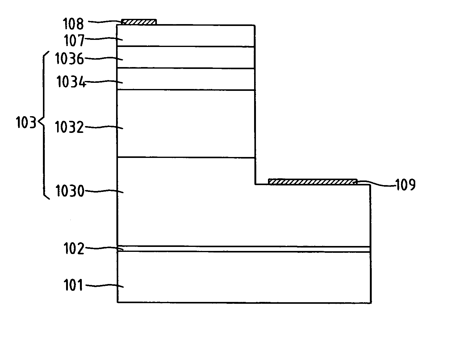
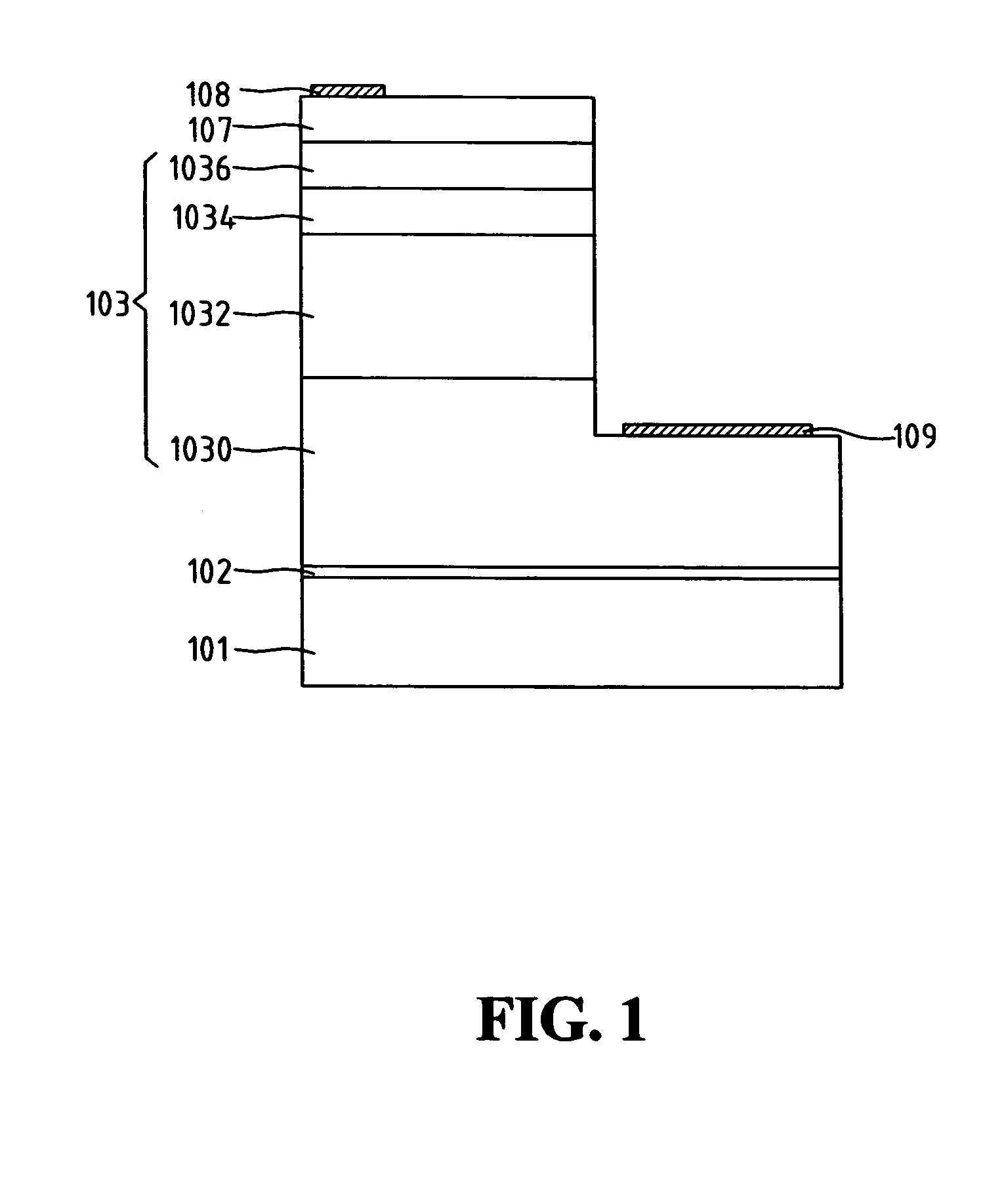
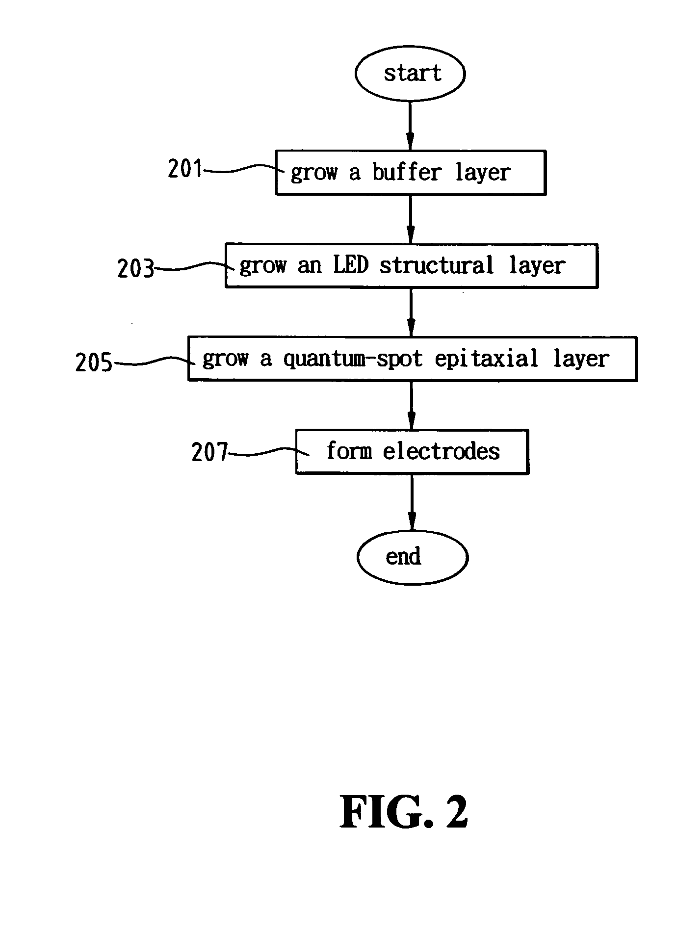
[0013]FIG. 1 is a schematic view showing the structure of LED according to an embodiment of the present invention. A sapphire substrate 101, which is made of SiC, Si, GaAs, LiAlO2, LiGaO2, or AlN, is put in a MOCVD (Metal Organic Chemical Vapor Deposition) system.

[0014] A GaN buffer layer 102 of 20-50 nm thick is formed firstly on the substrate 101 in 500-600° C. vapor, then an LED structural layer 103 on the buffer layer 102. The LED structural layer 103 comprises an n-type GaN layer 1030, a multiple-quantum-well structural layer 1032, a p-type GaAlN layer 1034, and a p-type GaN layer 1036, in which the n-type GaN layer 1030 grown on the buffer layer 102 is a GaN-based compound of group III-V.

[0015] The n-type GaN layer 1030 is a 1-2 μm thick Si-impurity-doped layer made in GaN-based compound semiconductor and grown by raising temperature of the substrate to 10000-1200° C. The test piece is then drawn out and dipped in the MOCVD system and the substrate 101 is heated to 700-900° ...


PUM

PropertyMeasurementUnit
critical angleaaaaaaaaaa
refractive indexaaaaaaaaaa
thickaaaaaaaaaa

Abstract

A light emitting diode (LED) structure and manufacture method thereof are disclosed, wherein a buffer layer is grown on a substrate and then an LED structural layer is grown on the buffer layer. The LED structural layer comprises a p-type quantum-dot epitaxial layer on a p-type GaN layer. As the p-type quantum-dot epitaxial layer has a coarsening and scattering effect, the path of light emitted from an INGaN multiple-quantum-well structural layer is changed. Therefore, it is possible to lessen the probability of total reflection and thereby heighten the light-emitting efficiency of LED.

Description

BACKGROUND OF THE INVENTION [0001] 1. Field of the Invention [0002] The present invention relates to light-emitting diodes (LEDs) structures, and more particularly, to an LED structure containing a p-type quantum-spot epitaxial layer grown on a p-type GaN layer. The present invention also relates to a manufacture method for the LED. [0003] 2. The Prior Art [0004] Because the refractive index (n) of gallium nitride (GaN) semiconductor as an LED material is 2.3 approximately, far different from that of air (n=1), a small critical angle of total reflection about 25° is resulted to block almost all the incident rays emitted from a light-emitting layer of LED. [0005] For improvement, a known method according to IEEE Transactions on Electron Devices, 47(7), 1492, 2000 was presented to coarsen a semiconductor surface, particularly an epitaxy surface to raise the scattering and refracting probability of incident light usually by way of etching. U.S. Pat. No. 5,040,044 discloses a chemical e...

Claims


Application Information

Patent Timeline
Patent Type & Authority Applications(United States)
IPC IPC(8): C30B1/00H01L29/06H01L33/00H01L33/32
CPCB82Y10/00B82Y30/00Y10S977/95H01L33/32H01L33/007
Inventor CHIEN, FEN-RENCHEN, LUNG-CHIEN
Owner FORMOSA EPITAXY INCORPORATION
Why Eureka
Try Eureka