Non-volatile semiconductor memory device

a semiconductor memory and non-volatile technology, applied in the direction of semiconductor devices, electrical devices, transistors, etc., can solve the problems of large bird's beak, difficult further large thinning of the layer, etc., to achieve large capacitance coupling and large capacitance coupling

Inactive Publication Date: 2005-02-10
KK TOSHIBA
View PDF5 Cites 15 Cited by
  • Summary
  • Abstract
  • Description
  • Claims
  • Application Information

AI Technical Summary

Benefits of technology

[0015] It is therefore a primary object of the present invention to provide a non-volatile semiconductor memory device including an inter-layer insulating layer, which is capable of ensuring even a large capacitance coupling between a control gate and a floating gate while securing an electric field relieving effect and a leak preventive function.
[0016] According to the present invention, a silicon nitride layer having a trap level density well lower than that of a silicon nitride layer formed by a normal CVD (Chemical Vapor Deposition), especially LPCVD (Low Pressure Chemical Vapor Deposition) method, is provided in the inter-layer insulating layer, whereby a large capacitance coupling between a control gate and a floating gate can be ensured by making an effective thickness of an oxide layer smaller than in the prior art while exhibiting an electric field relieving effect and a lead reducing effect. Furthermore, if such a silicon nitride layer is disposed contiguously to the control gate or the floating gate, an intrusion of a bird's beak can be restrained from occurring in a post-oxidation step, and it is therefore feasible to ensure the large capacitance coupling between the control gate and the floating gate.

Problems solved by technology

There arise the following problems inherent in the inter-layer insulating layer based on the ONO structure described above.
However, further thinning of the layer becomes difficult.
Especially when the silicon oxide layer 5a disposed directly on the floating gate is provided by a CVD (Chemical Vapor Deposition) method, a characteristic of density thereof is inferior to a thermal oxide layer, and hence oxygen diffuses fast within the layer, with the result that a large bird's beak occurs.
In the case of obtaining the silicon oxide layer at a low process temperature, the silicon oxide layer formed by the CVD method might be used more often than by the thermal oxidation, and therefore, in such a case, the intrusion of the bird's beak turns out a problem.

Method used


Image

  • Non-volatile semiconductor memory device
  • Non-volatile semiconductor memory device
  • Non-volatile semiconductor memory device

Examples


first embodiment

[0022] First Embodiment

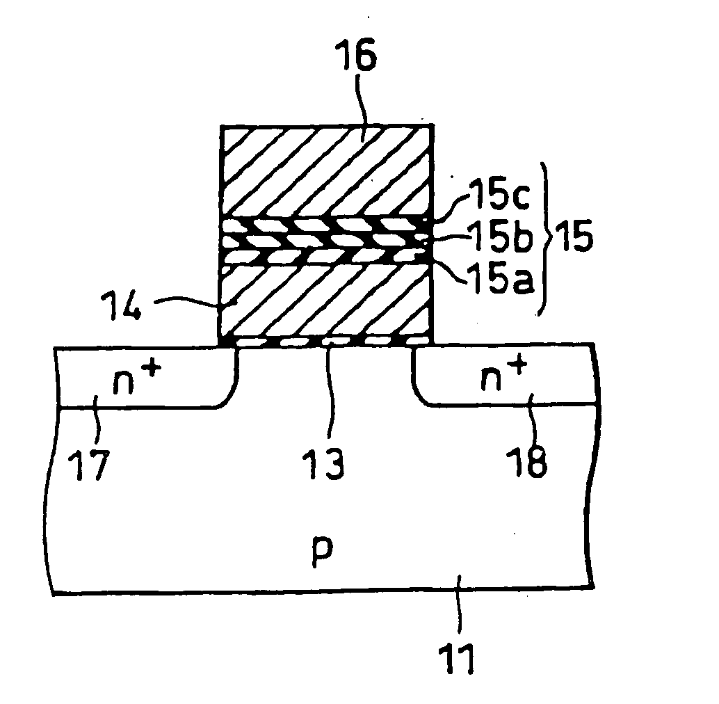
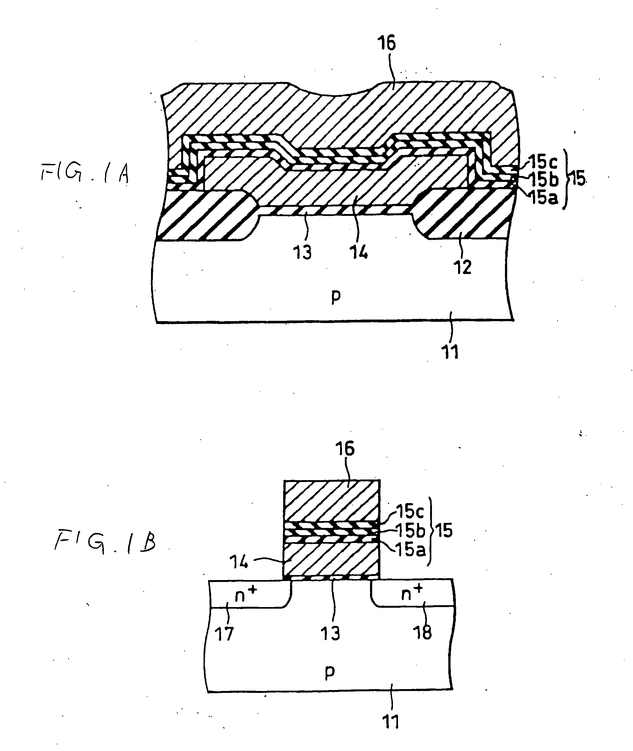
[0023]FIGS. 1A and 1B are sectional views taken in direction orthogonal to each other, showing a memory cell structure of a non-volatile semiconductor memory device in a first embodiment of the present invention. An element isolation insulating layer 12 is provided on a p-type silicon substrate 11, and a floating gate 14 composed of a polycrystalline silicon layer is provided through a tunnel insulating layer 13 on a device area defined by the element isolation insulating layer 12. The tunnel insulating layer 13 is classified as a silicon oxide layer. A control gate 16 composed of a polycrystalline silicon layer is stacked on the floating gate 14 via an inter-layer insulating layer 15. Source / drain diffused layers 17, 18 are so provided on the substrate as to be self-aligned with the control gate 16.

[0024] The inter-layer insulating layer 15 includes a silicon oxide layer 15a contiguous to the floating gate 14, and double-layered silicon nitride layers 15b, 1...

second embodiment

[0031] Second Embodiment

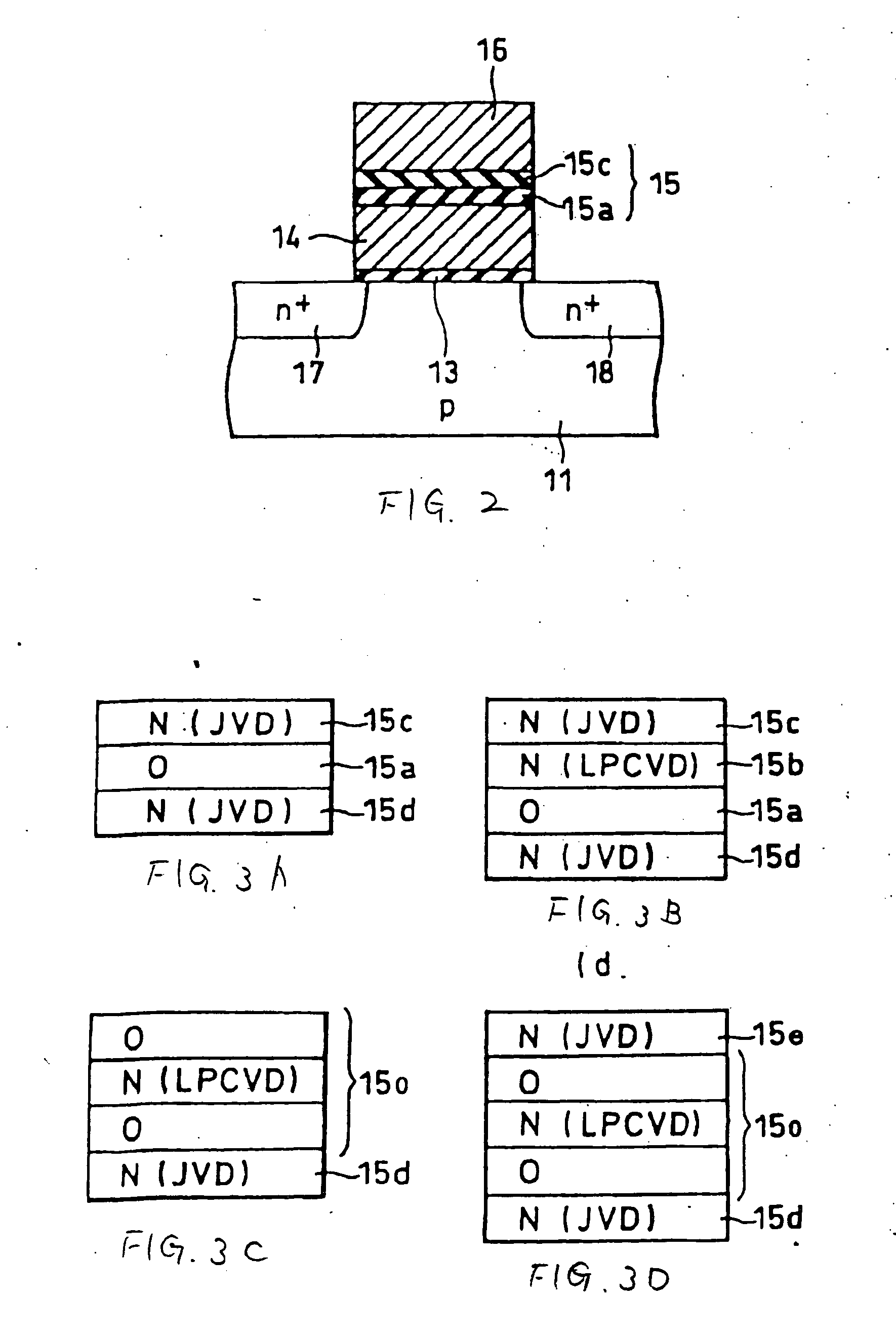
[0032]FIG. 2 shows, corresponding to FIG. 1B, a memory cell structure in a second embodiment of the present invention.

[0033] In the second embodiment of the present invention, the inter-layer insulating layer 15 is double-layered including two layers, i.e., from the side of the floating gate 14, the silicon oxide layer 15a and the silicon nitride layer 15c based on the JVD method which has a low trap density and a hydrogen content quantity on the order of 1019 / cm3 or less.

[0034] In the first embodiment, the silicon nitride layer 15b based on the LPCVD method and exhibiting the Frenkel-Poole type conduction, is disposed in the middle of the interlayer-insulating layer 15. If not operated with a high electric field, however, the silicon nitride layer 15b is not necessarily used. Namely, as shown in FIG. 2, for the purpose of blocking a defect in the lowermost silicon oxide layer 15a, the insulating layer may take a double-layered structure consisting of the s...

third embodiment

[0036] Third Embodiment

[0037] For preventing the bird's beak from intruding into the inter-layer insulting layer due to the post-oxidation, the silicon nitride layer formed by the JVD method and having a hydrogen content quantity on the order of 1019 / cm3 or less, is provided keeping its thickness as thin as approximately 3 nm directly on the floating gate (i.e., the lowermost layer of the inter-layer insulating layer) or just under the control gate (viz., the uppermost layer of the inter-layer insulating layer). If a layer based on the normal LPCVD method and exhibiting a high trap density is used as this silicon nitride layer, a threshold value of the memory cell might become unstable due to the trap and release of the electric charges within the layer. If the silicon nitride layer deposed by the JVD method and having a low trap density is used, however, the instability of the threshold value never occurs.

[0038]FIGS. 3A-3D show an extraction of only the structure of the inter-laye...


PUM


Abstract

A non-volatile semiconductor memory device according to the present invention has a semiconductor substrate and a memory cell having a floating gate provided through a tunnel insulating layer on the semiconductor substrate, and a control gate provided through an inter-layer insulting layer on said floating gate. The inter-insulating layer includes a silicon oxide layer contiguous to said floating gate, a first silicon nitride layer provided by a CVD method on the silicon oxide layer and a second silicon nitride layer provided on said first silicon nitride layer and having a lower trap density than that of the first silicon nitride layer. The inter-insulating layer may includes a silicon oxide layer contiguous to said floating gate and a silicon oxide layer deposited on said silicon oxide layer and having a quantity of hydrogen content on the order of 1019/cm3 or less. The inter-insulating layer also may includes a silicon oxide layer serving as a layer contiguous to at least one of the floating gate and the control gate, and having a lower trap density than that of a silicon nitride layer formed by a CVD method.

Description

BACKGROUND OF THE INVENTION [0001] 1. Field of the Invention [0002] The present invention relates to a non-volatile semiconductor memory device including a memory cell having a stacked gate structure. [0003] 2. Description of the Background Art [0004] What has hitherto been known as a non-volatile semiconductor memory device uses a memory cell structure on which a floating gate is provided through a tunnel insulating layer on a semiconductor substrate, and a control gate is stacked thereon through an inter-layer insulating layer. The inter-layer insulating layer of this memory cell normally involves the use of a so-called ONO (oxide-Nitride-oxide) structure composed of a silicon oxide layer, a silicon nitride layer and a silicon oxide layer. [0005]FIGS. 4A and 4B show sections, taken in two directions orthogonal to each other, of the memory cell structure described above. Normally in a flash memory, the control gate of the a plurality of memory cells are consecutively arranged and s...

Claims


Application Information

Patent Timeline
Patent Type & Authority Applications(United States)
IPC IPC(8): H01L21/28H01L21/8247H01L27/115H01L29/51H01L29/788H01L29/792
CPCH01L21/28273H01L29/42324H01L29/7881H01L29/513H01L29/511H01L29/40114H10B69/00
Inventor MORI, SEIICHI
Owner KK TOSHIBA
Why Eureka
Try Eureka