Analysis and monitoring of stresses in embedded lines and vias integrated on substrates

a technology of embedded lines and vias, which is applied in the direction of force measurement by measuring optical property variation, semiconductor/solid-state device testing/measurement, instruments, etc., can solve the problems of complex stress state of each device feature, adversely affecting the integrity or effectiveness of subsequent processing steps, or the performance and reliability of the device under such stress, and achieves the effect of improving the overall yield

Inactive Publication Date: 2005-02-10
CALIFORNIA INST OF TECH
View PDF9 Cites 43 Cited by
  • Summary
  • Abstract
  • Description
  • Claims
  • Application Information

AI Technical Summary

Benefits of technology

During fabrication of one or more wafers, changes in stresses on a wafer may be caused by, for example, thermal cycling or a transition from one processing step to another during fabrication. Therefore, a system may be designed based on the analytical computations to provide in-situ and real time monitoring of stresses in wafers because the analytical expressions described here allow for fast p

Problems solved by technology

Hence, the interfacing of different materials and different structures may cause a complex stress state in each device feature due to differences in the material properties, e.g., either or both of mechanical and thermal properties.
Stresses caused by

Method used


Image

  • Analysis and monitoring of stresses in embedded lines and vias integrated on substrates
  • Analysis and monitoring of stresses in embedded lines and vias integrated on substrates
  • Analysis and monitoring of stresses in embedded lines and vias integrated on substrates

Examples


Embodiment Construction

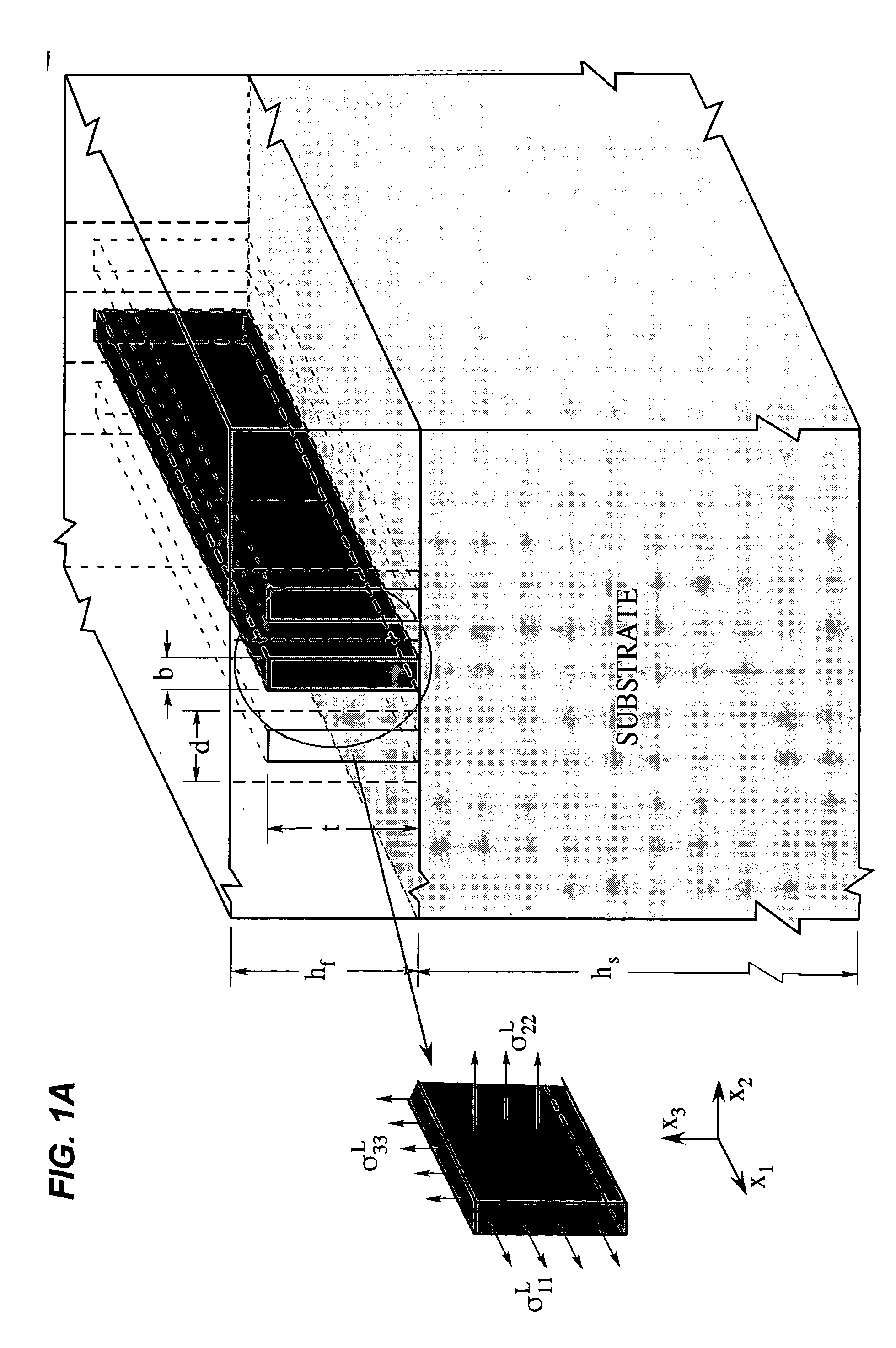
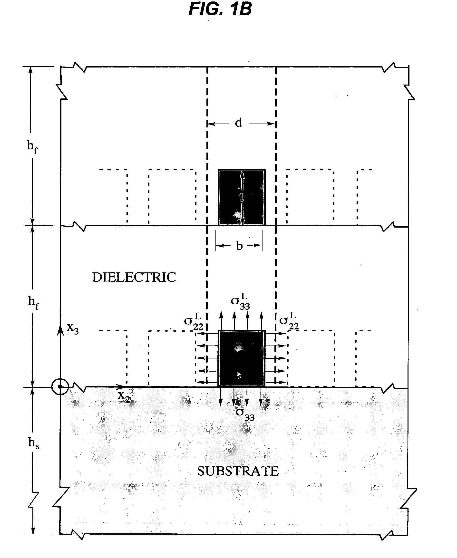
FIGS. 1A and 1B show geometries representative of exemplary integrated structures for the analytical computations and expressions of stresses described based on a thermoelastic composite analysis. FIG. 1A shows one layer with embedded, parallel tall line features formed on a thick substrate. FIG. 1B shows a multi-layer structure having two or more layers with embedded, parallel line features over the substrate. In general, such a multi-layer structure has n layers where a 2-layer example for n=2 is illustrated in FIG. 1B. A Cartesian coordinate system (x1,x2,x3) is shown in the insert. The directions marked as x1 and x2 represent two orthogonal directions parallel to the substrate where the direction x1 is along the longitudinal direction of the line features in the layer and the direction x2 is perpendicular to the line features. The direction marked as x3 represents the direction normal to the plane of the substrate.

In each layer for a multi-layer structure, the embedded line fea...


PUM


Abstract

Techniques and systems for applying analytical computations of stresses to layers with embedded line features to obtain stress information, to design microstructures, and to design and control fabrication processes.

Description

This application relates to stresses in device features fabricated on substrates including integrated structures having multiple layers. Substrates formed of suitable solid-state materials may be used as platforms to support various structures, such as multilevel, thin film microstructures deposited on to the substrates. Integrated electronic circuits, integrated optical devices and opto-electronic circuits, micro-electro-mechanical systems (MEMS), and flat panel display systems (e.g., LCD and plasma displays) are examples of such structures integrated on various types of substrates. Substrates may be made of a semiconductor material (e.g., silicon wafers), silicon on insulator wafer (SOI), a glass material, and others. Different material layers or different structures may be formed on the same substrate in these structures and are in contact with one another to form various interfaces. Some devices may also use complex multilayer or continuously graded geometries and may form var...

Claims


Application Information

Patent Timeline
IPC IPC(8): B81C99/00G01B9/02G06F7/60G06F17/10G06G7/48G06G7/50H01LH01L21/66H01L21/768
CPCH01L21/768B81C99/004H01L22/00
Inventor ROSAKIS, ARES J.PARK, TAE-SOONSURESH, SUBRA
Owner CALIFORNIA INST OF TECH
Why Eureka
Try Eureka