Via array monitor and method of monitoring induced electrical charging

Inactive Publication Date: 2005-02-10
TAIWAN SEMICON MFG CO LTD
View PDF8 Cites 39 Cited by
  • Summary
  • Abstract
  • Description
  • Claims
  • Application Information

AI Technical Summary

Benefits of technology

[0010] To achieve the foregoing and other objects, and in accordance with the purposes of the present invention, as embodied and broadly described herein, the present invention provides a via array monitor and method for determining and reducing an electrically charged state of a semiconductor process wafer.
[0011] In a first embodiment, the method includes providing a metal filled via array in at least one level of multi-level device comprising a semiconductor process wafer the metal filled via array in electrical communication with at least one underlying metallization layer the metal filled via array further including

Problems solved by technology

In addition, the use of pure copper in lower metallization levels creates the potential of diffusion of copper through dielectric insulating layers and poisoning of doped silicon well areas in transistors by creating deep impurity levels and contributing to junction leakage.
As design rule technology progresses below 0.25 microns, also referred to as sub-quarter micron technology, the ability to achieve complete overlap of metal interconnect lines and underlying metal filled vias is increasingly problematical.
Typically, complete overlap is not generally achievable, causing the underlying metal filled via to be partially exposed after forming the overlying metal lines, for example AlCu metal lines formed by a metal etch process.
One problem with etching overlying metal layers, for example AlCu, in a reactive ion etch (RIE) process is the exposure of a portion of t

Method used


Image

  • Via array monitor and method of monitoring induced electrical charging
  • Via array monitor and method of monitoring induced electrical charging
  • Via array monitor and method of monitoring induced electrical charging

Examples


Embodiment Construction

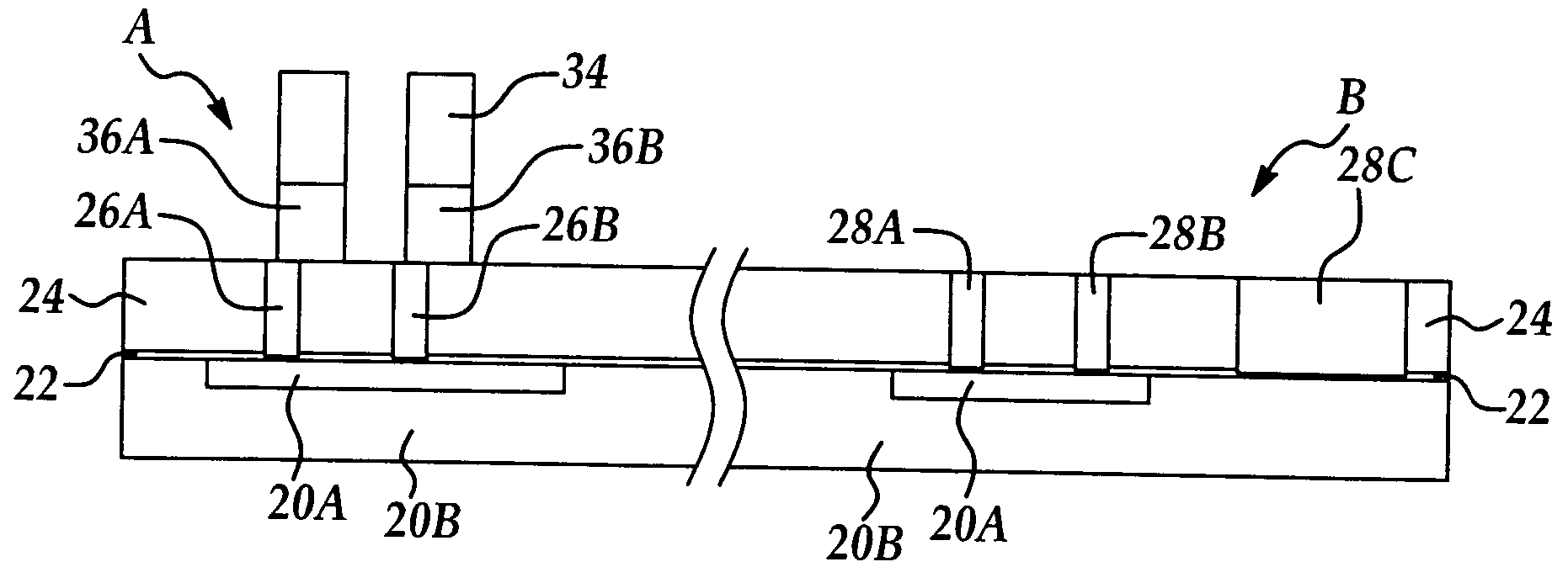
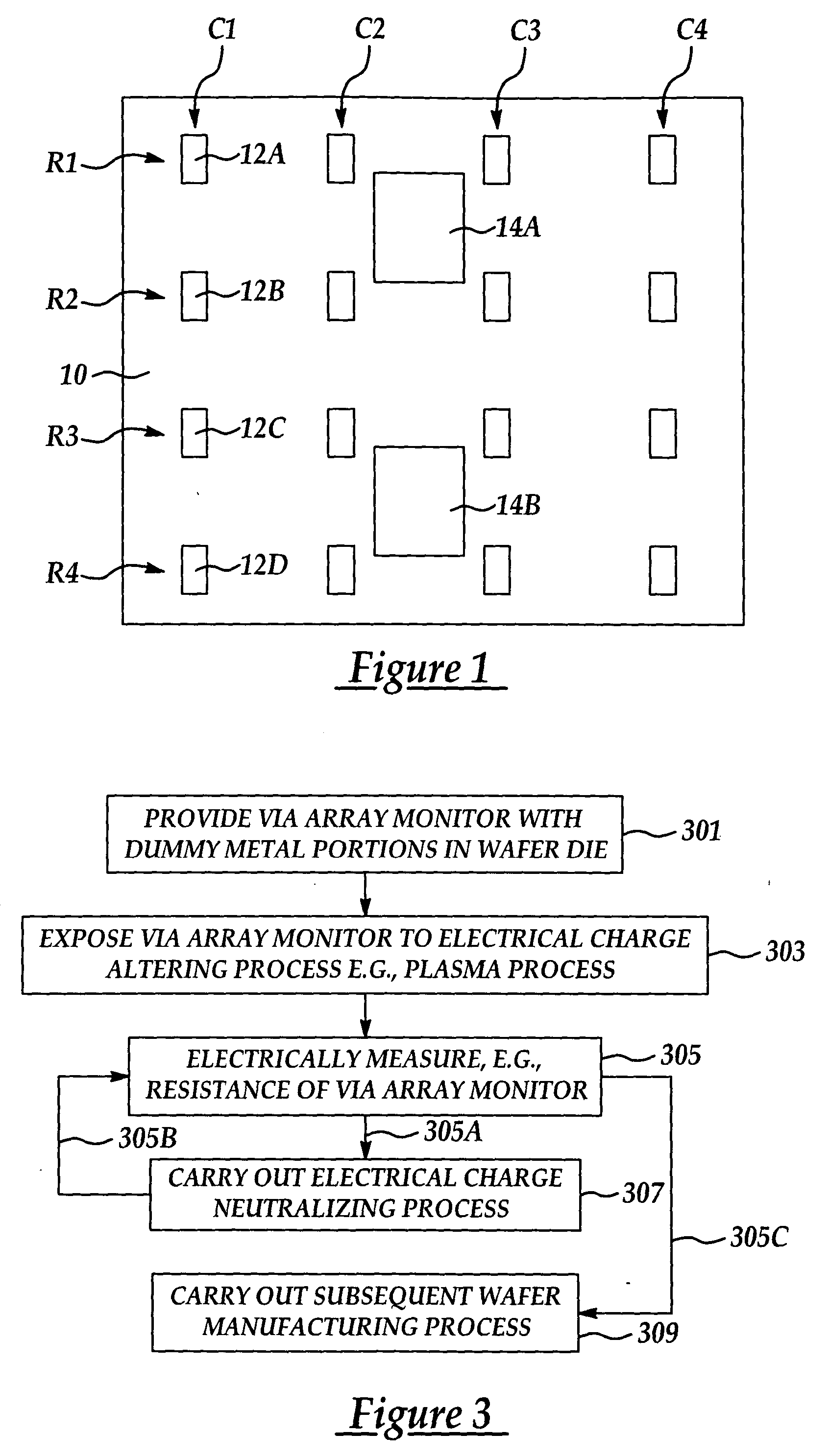
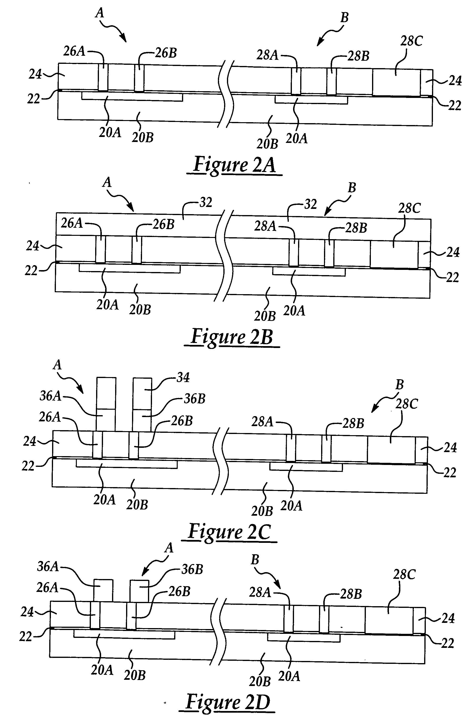
[0016] Although the method and via array electrical monitor of the present invention is explained by reference to parallel formation of tungsten plugs (vias) with an overlying AlCu metal interconnect structure, it will be appreciated that the via array monitor may be formed of any metal in parallel with an micro-integrated circuit manufacturing process to advantageously monitor the electrical properties including an electrical charge state of a substrate following any charge imbalance producing manufacturing process. For example, charge imbalance producing manufacturing process may include plasma enhanced treatments such as reactive ion etch (RIE) processes, CMP treatments, as well as exposure to electrical charge producing (e.g., UV) light environments. In accordance with the exemplary embodiment of the invention, it is noted that the via array monitors are particularly advantageously used in monitoring an electrical charge state of the wafer process surface where tungsten vias are...


PUM


Abstract

An electrical monitor comprising a via array and method for determining and reducing an electrically charged state of a semiconductor process wafer the method including providing a metal filled via array including a plurality of interspersed electrically isolated dummy metal portions to form a via array monitor; exposing the semiconductor process wafer including the via array monitor to an electrical charge altering process including to produce an electrically charged state over at least a portion of the semiconductor wafer; carrying out electrical measurements of the via array monitor to determine a level of the electrically charged state; and, carrying out an electrically charge neutralizing process to reduce a level of the electrically charged state to a predetermined acceptable level prior to carrying out a subsequent process.

Description

FIELD OF THE INVENTION [0001] This invention generally relates to micro-integrated circuit processing methods including and more particularly to wafer manufacturing process induced electrical charging such as plasma induced charging and an electrical monitoring structure and method to determine electrical properties including an electrical charge state of the process wafer to reduce or avoid circuitry defects including galvanic corrosion of tungsten plugs to improve device reliability and performance. BACKGROUND OF THE INVENTION [0002] Metallization interconnects are critical to the proper electronic function of semiconductor devices. Several advances in semiconductor processing have been aimed at improving signal transport speed by reducing metal interconnect resistivities and improving electromigration resistance. Copper has increasingly found application for use as metal interconnects in upper levels of a multi-level device due to its low resistivity and higher resistance to elec...

Claims


Application Information

Patent Timeline
IPC IPC(8): H01L21/66H01L23/544
CPCH01L22/20Y10S438/926H01L2924/3011H01L22/34
Inventor HSU, YUNG-LUNGWU, JAMES
Owner TAIWAN SEMICON MFG CO LTD
Why Eureka
Try Eureka