Monoatomic and moncrystalline layer of large size, in diamond type carbon, and method for the manufacture of this layer

a monoatomic and monocrystalline technology, applied in the field of monoatomic and monocrystalline layer of diamond type carbon, can solve the problems of limited use of diamonds in the industry, rare and expensive diamonds in the natural state, and relatively low dimensions of natural diamonds availabl

Inactive Publication Date: 2005-02-17
COMMISSARIAT A LENERGIE ATOMIQUE ET AUX ENERGIES ALTERNATIVES +1
View PDF4 Cites 7 Cited by
  • Summary
  • Abstract
  • Description
  • Claims
  • Application Information

AI Technical Summary

Problems solved by technology

Diamond exists in the natural state but is very rare and expensive.
Furthermore, the natural diamonds available have relatively low dimensions, which limits their use in industry, their main outlet remaining jewellery.
It is ...

Method used


Image

  • Monoatomic and moncrystalline layer of large size, in diamond type carbon, and method for the manufacture of this layer
  • Monoatomic and moncrystalline layer of large size, in diamond type carbon, and method for the manufacture of this layer

Examples


Embodiment Construction

[0009] The aim of the present invention is to rectify the above inconveniences and, in order to do this, to suggest a structure having electronic, chemical and structural properties close to those of diamond, which will make it possible to obtain a base on which the growth of layers of diamond can take place under the same conditions: the same chemical element (carbon), the same electronic properties (sp3 configuration), and the lowest possible lattice discrepancy between the substrate and the crystal of diamond.

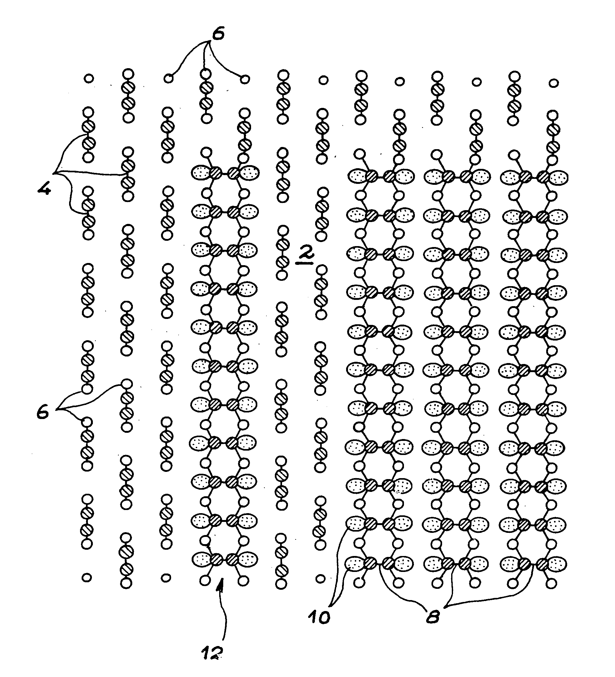
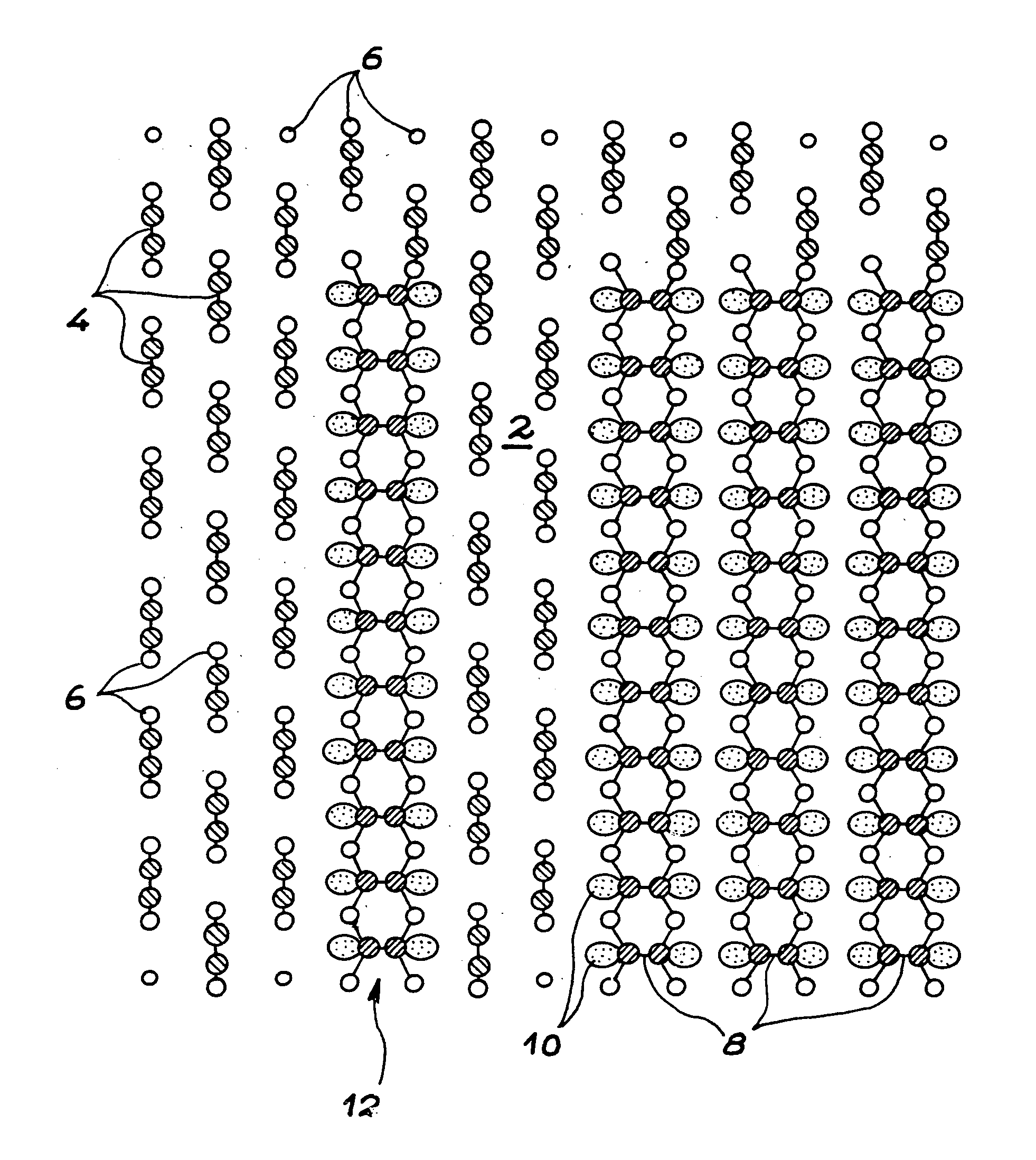
[0010] To be precise, the present invention has the aim of a monoatomic and monocrystalline layer of carbon of the diamond type, this layer being characterised in that it is formed on the surface of a monocrystalline substrate in SiC and extends closely over the totality of this substrate.

[0011] According to a first special embodiment of the monoatomic layer and monocrystalline layer, the aim of the invention, the monocrystalline substrate in SiC is a thin layer of monocry...


PUM


Abstract

Monoatomic and monocrystalline layer of large size, in diamond type carbon, and method for the manufacture of this layer.
According to the invention, a monocrystalline substrate (2) is formed in SiC terminated by an atomic plane of carbon according to a reconstruction c(2x2) and at least one annealing is carried out, capable of transforming this atomic plane, which is a plane of dimers C≡C (4) of sp configuration, into a plane of dimers C-C (8) of sp3 configuration. Application to microelectronics, optics, optoelectronics, micromechanics and biomaterials.

Description

TECHNICAL FIELD [0001] The present invention relates to a monoatomic and monocrystalline layer of diamond type carbon, as well as a method for manufacturing said layer. STATE OF THE PRIOR ART [0002] Diamond exists in the natural state but is very rare and expensive. Furthermore, the natural diamonds available have relatively low dimensions, which limits their use in industry, their main outlet remaining jewellery. [0003] This has led to research on methods for artificial production of diamond. [0004] In fact, diamond is far and away the best semiconductor possible for the electronics industry. It outclasses silicon and the semiconductor compounds III-V by at least four times in terms of quality factor (in particular as far as rapid electronics, high powers and high temperatures are concerned). [0005] It is also a biocompatible material and is very hard. [0006] However, in order to use it, it is imperative to have available monocrystals of diamond of sufficient size, especially in th...

Claims


Application Information

Patent Timeline
IPC IPC(8): C30B1/00C30B29/04C30B1/10C30B33/00H01L29/16
CPCC30B1/00C30B33/00H01L29/16H01L29/1602Y10S117/902C30B29/04C30B29/36
Inventor DERYCKE, VINCENTDUJARDIN, GERALDMAYNE, ANDREWSOUKIASSIAN, PATRICK
Owner COMMISSARIAT A LENERGIE ATOMIQUE ET AUX ENERGIES ALTERNATIVES
Why Eureka
Try Eureka