

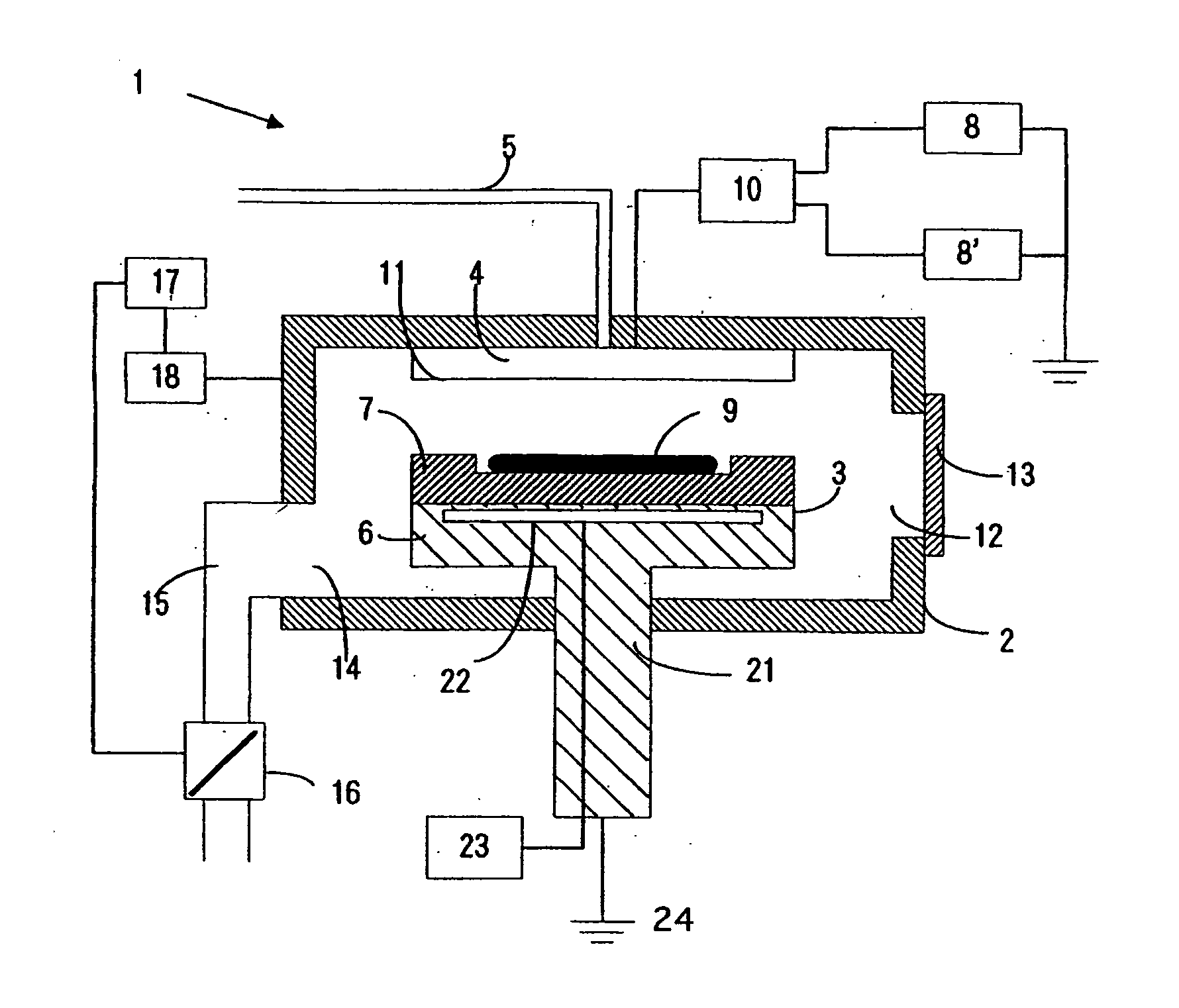
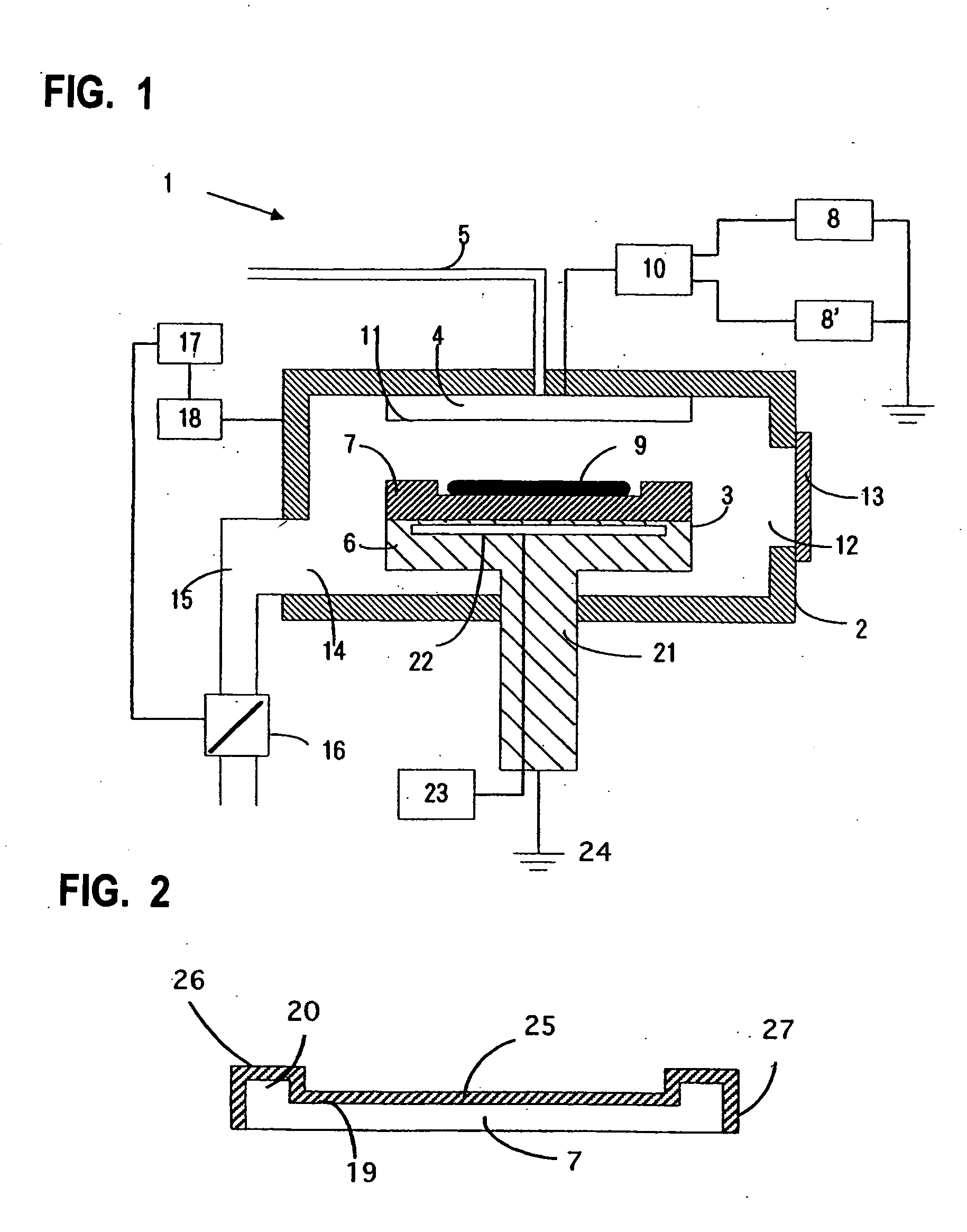
Semiconductor substrate supporting apparatus
a technology of semiconductor apparatus and supporting apparatus, which is applied in the direction of coating, metallic material coating process, chemical vapor deposition coating, etc., can solve the problems of frequent charge-up damage of semiconductor apparatus, insufficient resistance of aluminum-alloy surface, and leakage current, etc., and achieve the effect of small leakage curren
- Summary
- Abstract
- Description
- Claims
- Application Information
AI Technical Summary
Benefits of technology
Problems solved by technology
Method used
Image

Examples
examples
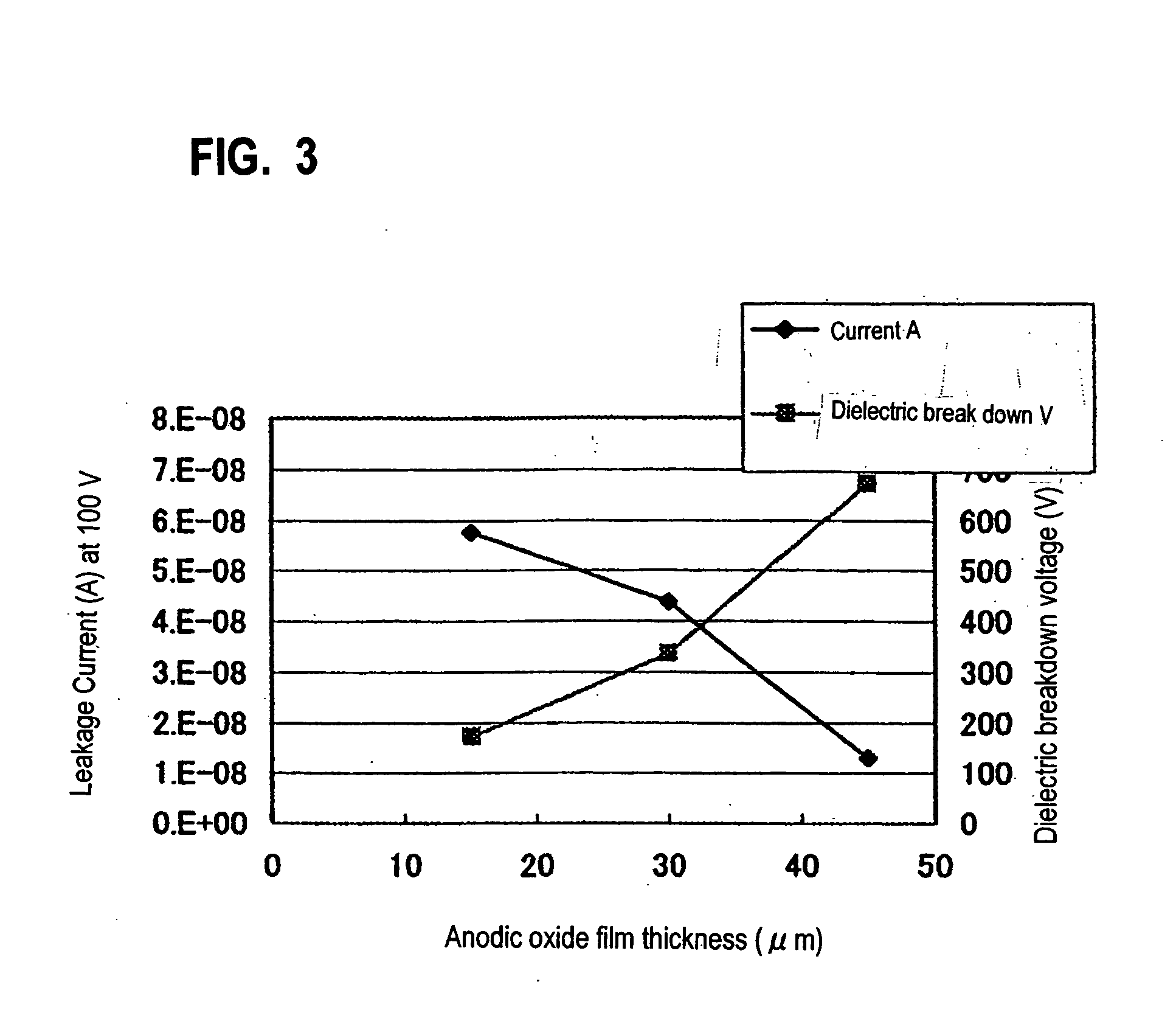
[0054] Measurements conducted for evaluating electrical characteristics of the substrate supporting apparatus according to an embodiment of the present invention are described below. Measurements were made using the substrate supporting apparatuses respectively having anodic oxide film thicknesses of 15 μm, 30 μm and 45 μm. By placing an electrode with a diameter of 0.17 mm over the substrate supporting apparatus and by applying a direct-current voltage of 0-1000 V, a leakage current and a voltage generating dielectric breakdown were measured. Measurement results of leakage current values and dielectric breakdown voltage values are shown in Table 1. Incidentally, in this example, an IV measuring instrument for measuring leakage current for wafers was used, wherein instead of a wafer, a placing block was placed, and instead of a film formed on the wafer, an anodic oxide film formed on the placing block was analyzed.
TABLE 1Thickness ofLeakage Current ValueDielectricAnodic Oxidewhen ...
PUM
| Property | Measurement | Unit |
|---|---|---|
| Thickness | aaaaa | aaaaa |
| Thickness | aaaaa | aaaaa |
| Thickness | aaaaa | aaaaa |
Abstract
Description
Claims
Application Information