Stamp having an antisticking layer and a method of forming of repairing such a stamp

a technology of anti-sticking layer and stamp, which is applied in the field of stamp having an anti-sticking layer and a forming method of repairing such a stamp, can solve the problems of insufficient stability of film, deterioration of film quality in embossing, and damage to the stamp reproduced on the plate, so as to achieve stable anti-sticking layer, easy to recreate anti-sticking properties, and more sensitive to sticking

Inactive Publication Date: 2005-02-24
OBDUCAT AB SE
View PDF3 Cites 85 Cited by
  • Summary
  • Abstract
  • Description
  • Claims
  • Application Information

AI Technical Summary

Benefits of technology

nge of 1-100 micrometers. The best effect of the invention is achieved with structures within the range of submicrometers since such structures are relatively more sensitive to sticking when releasing the stamp.
The present invention is based on the discovery that a stable antisticking layer can be provided on the surface of the stamp by attaching molecular chains to the stamp which have antisticking properties. The molecular chains are formed in such a manner that the antisticking properties can easily be recreated when the antisticking layer is worn after being used for some time.
The surface of the stamp is conveniently made of a material M which is suitable for producing nanostructured patterns. Examples of such materials M are Si, Al, Ti, Ni, Cr and oxides thereof. Si is particularly suitable since it has satisfactory hardness and is easy to work when forming patterns in nanoscale. If the surface is made of metal, such as Al, Ti, Cr, Ni, it is normally preferable for the surface to have an oxide layer. To obtain a stronger oxide layer, the surface can be oxidised, for instance by means of an oxygen plasma. In some metals, such as Ni, Cr, it is particularly suitable to generate such a stronger oxide layer.
According to a preferred embodiment of the invention, a first and a second reagent are used. The first reagent is bound in a first reaction to the surface of the stamp, whereas the second reagent is bound in a second reaction to the first reagent. The reason why this embodiment is preferred is that it is relatively easy to obtain commercially available compounds which can suitably be used as first and second reagents.
A first reagent to be used in manufacturing the stamp according to the invention has at least two functional groups. A first functional group is intended to bind to the surface of the stamp. One example of such a f

Problems solved by technology

Also the pattern replicated on the plate can be damaged by such sticking.
According to Jaszewski et al.

Method used


Image

  • Stamp having an antisticking layer and a method of forming of repairing such a stamp
  • Stamp having an antisticking layer and a method of forming of repairing such a stamp
  • Stamp having an antisticking layer and a method of forming of repairing such a stamp

Examples


example 1

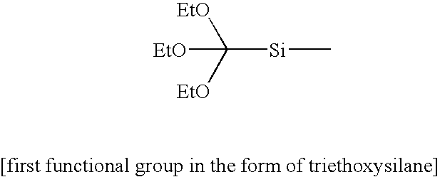
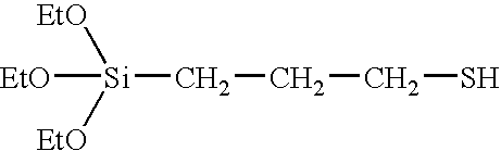
A stamp made of silicon was etched to form a nanostructured pattern. The stamp was washed with, in succession, trichloroethylene, ethanol and isopropanol. The stamp was subsequently dipped into a beaker with hexane at room temperature with 0.2% mercaptopropyltriethoxysilane, which corresponded to an excess amount of mercaptopropyltriethoxysilane, and was allowed to react for 4 h. The stamp was then removed from the beaker and cleaned with, in succession, trichloroethylene, ethanol and isopropanol. The stamp was dried and subsequently placed in a beaker, which contained hexane at room temperature with 2% 1H, 1H, 2H, 2H-perfluorooctanethiol. After 16 h, the stamp was removed from the vessel, washed with hexane in three successive baths and then dried. The stamp was tested in a nanoimprint lithography process and was found to resist 50 embossings without any particular signs of wear being detected.

example 2

A stamp made of silicon was patterned and washed in the manner described in Example 1. The stamp was subsequently placed in an oven, which had a temperature of 200° C. and was evacuated to a pressure of 1 kPa. Mercaptopropyltriethoxysilane was injected in large excess into the oven and vaporised. The stamp was allowed to react with the mercaptopropyltriethoxysilane for 3 h and was then removed from the oven and allowed to cool. The stamp was cleaned and treated with 1H, 1H, 2H. 2H-perfluorooctanethiol in liquid phase in the manner described in Example 1. The stamp was tested in a nanoimprint lithography process and was found to resist 50 embossings without any particular signs of wear being detected.

example 3

The experiment in Example 2 was repeated with materials and reagents according to Table 1:

TABLE 1Combinations of materials and compounds used in Example 3.Surface ofthe stampFirst reagentSecond reagentSi(MeO)3Si(CH2)3NH2Cl(C═O)(CH2)2C(CF3)3SiCl3Si(CH2)3SHSH(CH2)2(CF2)7CF3Si(EtO)3Si(CH2)3OHHO(C═O)(CH2)2(CF2)2CF3Al(MeO)3Si(CH2)3SHSH(CH2)2(CF2)5CF3AlCl3Si(CH2)3SHSH(CH2)2(CF2)2CF3Ni*(EtO)3Si(CH2)3SHSH(CH2)2(CF2)5CF3Ti(EtO)3Si(CH2)3SHSH(CH2)2(CF2)5CF3

*The surface of Ni was first treated with an oxygen plasma to oxidise the surface.

The finished stamps were tested in a nanoimprint lithography process and all of them were found to resist 50 embossings without any particular signs of wear being detected.


PUM

PropertyMeasurementUnit
Lengthaaaaaaaaaa

Abstract

A stamp for use in transferring a pattern in nano-scale has a monomolecular antisticking layer. The anti-sticking layer comprises molecular chains, which are covalently bound to the surface of the stamp and which each comprise at least one fluorine-containing group. Each molecular chain contains a group Q, which comprises a bond which is weaker than the other bonds in the molecular chain as well as the covalent bond that binds the molecular chain to the surface of the stamp. Splitting of said bond in the group Q creates a group Q1, which is attached to the part of the molecular chain being left on the surface of the stamp and which is capable of reacting with a fluorine-containing compound to restore the antisticking layer. In a method of manufacturing a stamp for use in transferring a pattern in nanoscale, the stamp is provided with the above-mentioned molecular chain. In a method of repairing a damaged antisticking layer of the above-mentioned stamp, the stamp is treated with a repairing reagent, which has a coupling end, which is capable of reacting with the group Q1, and a fluorine-containing group located at the other end of the repairing reagent.

Description

FIELD OF THE INVENTION The present invention relates to a stamp for use in transferring a pattern in nanoscale, which stamp has a monomolecular antisticking layer. The invention also relates to a method of manufacturing a stamp for use in transferring a pattern in nanoscale, which stamp has a monomolecular antisticking layer. The invention further relates to a method of repairing said monomolecular antisticking layer. BACKGROUND ART In the replication of nanostructures, use is often made of a stamp, which hot embosses a pattern into a plate coated with a suitable polymer, such as a thermoplastic. It is necessary to provide an antisticking boundary surface between the patterned stamp and the polymer to prevent thermoplastic from getting stuck to and contaminating the surface of the stamp when the stamp is released from the coated plate after embossing. Also the pattern replicated on the plate can be damaged by such sticking. For successful embossing, the stamp must thus be chemic...

Claims


Application Information

Patent Timeline
IPC IPC(8): B82B1/00B29C59/00B41C3/06B41M1/04B41M1/06B81C99/00G03F7/00H01L21/027
CPCB82Y10/00G03F7/0017G03F7/0002B82Y40/00
Inventor HEIDARI, BABAKLING, TORBJORN
Owner OBDUCAT AB SE
Why Eureka
Try Eureka