Double substrate reflective spatial light modulator with self-limiting micro-mechanical elements

a micro-mechanical element and spatial light modulator technology, applied in the field of spatial light modulators, can solve the problems of reducing optical efficiency, reducing the response time of the most widely used liquid crystal, and limited device contrast ratio, and achieves the effects of high device robustness, simple fabrication, and low cost and simple construction

Inactive Publication Date: 2005-02-24
TEXAS INSTR INC +1
View PDF70 Cites 55 Cited by
  • Summary
  • Abstract
  • Description
  • Claims
  • Application Information

AI Technical Summary

Benefits of technology

[0025] Since the two substrates are joined together only after they are individually fabricated, the fabrication processes for each substrate are decoupled. As there is no concern for CMOS compatibility during the manufacturing of the top substrate, an advantage of the spatial light modulator of this invention is that the mechanically deflectable reflective elements can be made from materials chosen only for their excellent mechanical properties, such as LPCVD-deposited silicon nitride, silicon oxide, amorphous silicon and poly-silicon. Since these films are deposited at high temperatures, they are not normally compatible with CMOS processes, because the latter use aluminum interconnects which would melt at these higher temperatures.
[0026] A further advantage of this spatial light modulator is that after the two substrates are bonded together, the moving parts may be fully encapsulated. This provides an excellent method of packaging and leads to high device robustness.
[0027] The spatial light modulator of this invention has the further advantage that it is inexpensive and straightforward to construct. It is composed of two substrates: one which may be made using standard CMOS techniques, and a second optically transmissive substrate containing the deflectable reflective elements, which is very simple to fabricate.
[0028] Yet anot

Problems solved by technology

However, such liquid crystal based devices have several disadvantages for SLM applications.
First, much of the light is absorbed in the polarizing filters, reducing optical efficiency.
In addition, the devices have limited contrast ratio, (the ratio of the intensities of the pixel when on and the pixel when off), and the response time of the most widely used liquid crystals is very slow (several milliseconds).
Liquid crystals also have poor performance outside a fairly narrow temperature range.
A disadvantage of the Eidophor system is that the oil film is polymerized by constant electron bombardment and oil vapors result in a short cathode lifetime.
A disadvantage of both of these systems is their use of bulky and expensive vacuum tubes.
Although the switching voltage of this SLM is lowered by connecting the deflectable mirror elements at only one corner, the device has low efficiency due to the small optically active area (as a fraction of the entire device area).
In addition, diffraction from the addressing circuitry lowers the contrast ratio of the display.
Aluminum has the disadvantage, however, of being susceptible to fatigue and plastic deformation, which can lead to long-term reliability problems and cell “memory”, where the rest position begins to tilt towards its most frequently occupied position.
Additional disadvantages of the DMD include: 1) A large dimple (caused by the mirror support post) is present at the center of the mirror in current designs which causes scattering of the incident

Method used


Image

  • Double substrate reflective spatial light modulator with self-limiting micro-mechanical elements
  • Double substrate reflective spatial light modulator with self-limiting micro-mechanical elements
  • Double substrate reflective spatial light modulator with self-limiting micro-mechanical elements

Examples


Embodiment Construction

[0083] This description refers to several figures which contain reference numerals. The same reference numerals in different figures indicate similar or identical items.

[0084] Throughout this description, the words “optical” and “light” are used. In the description and claims, “optical” means related to any electromagnetic frequencies, not just frequencies in the visible range. For example, an “optically transmissive substrate” is a substrate which is transmissive to electromagnetic propagation of a working frequency, whether in the visible range or not.

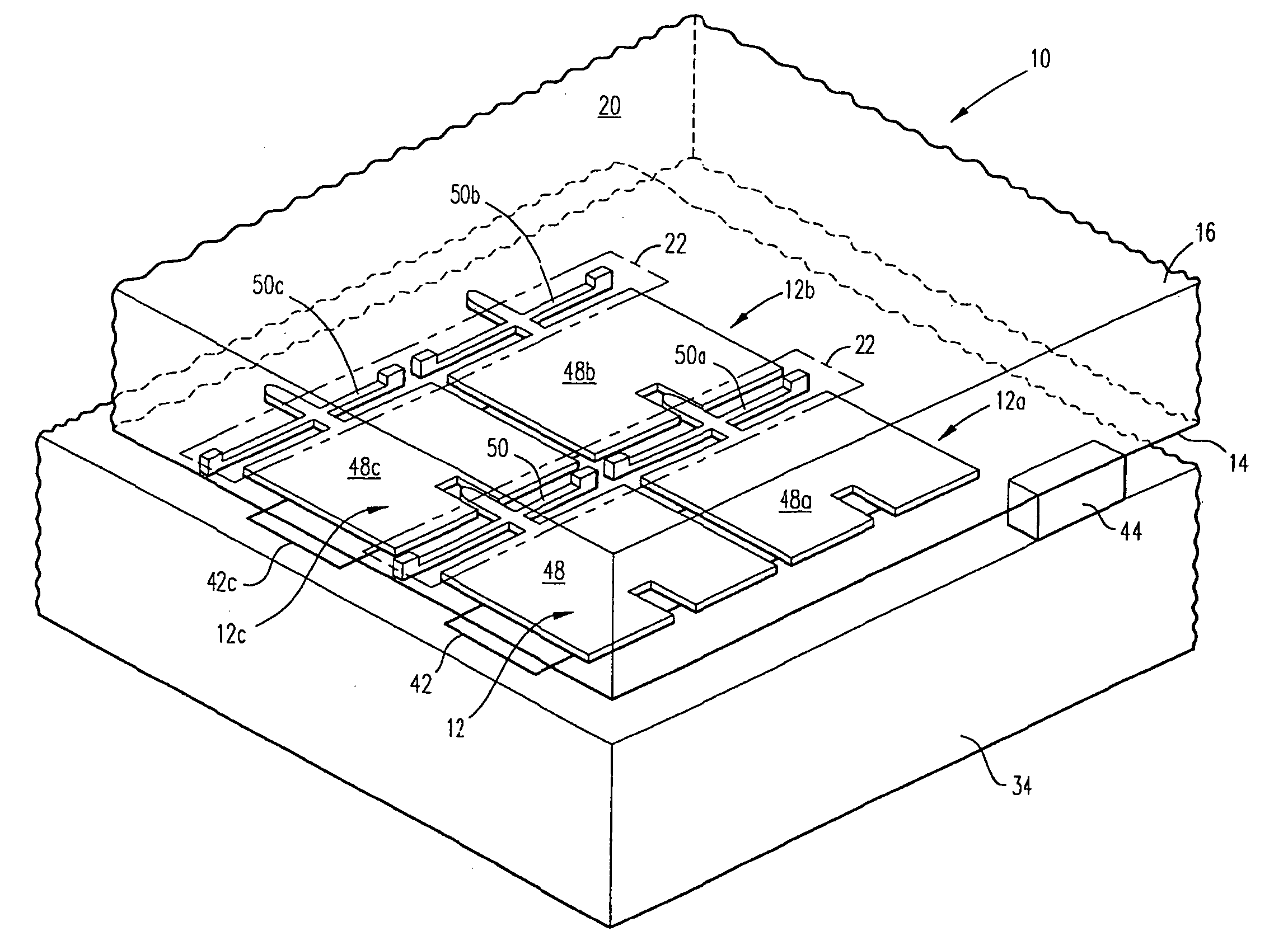
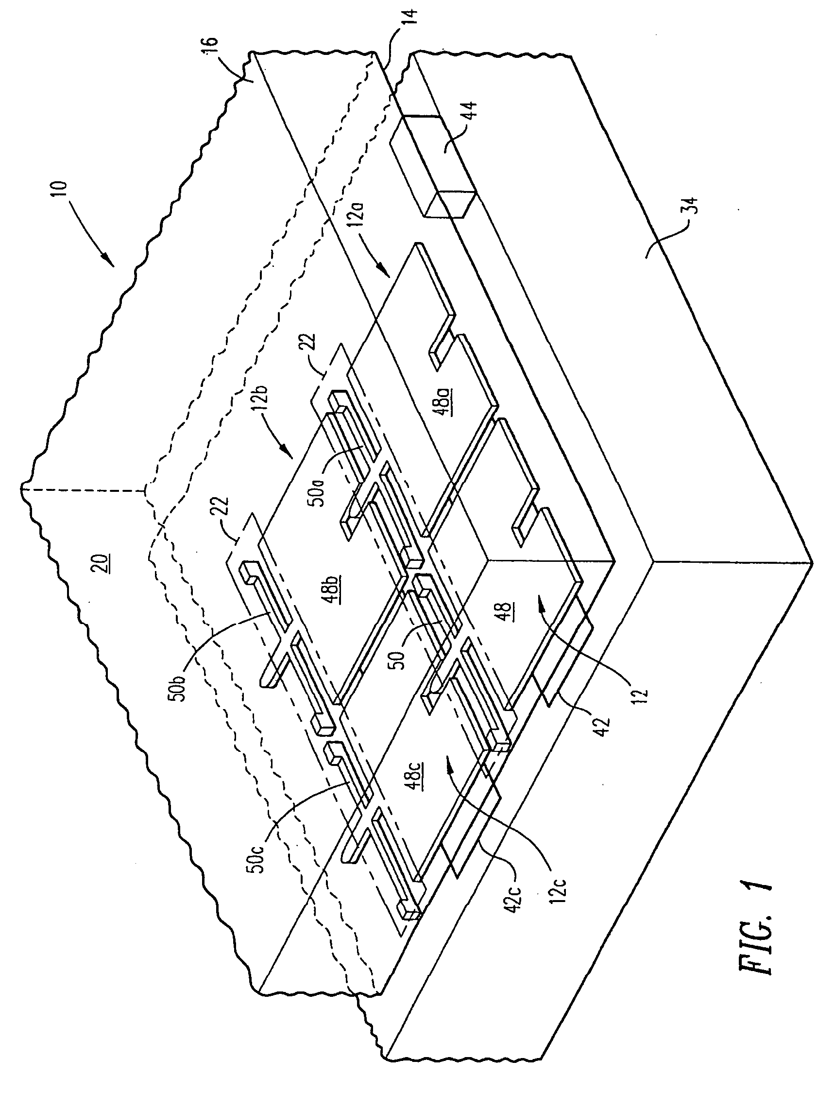
[0085] A top perspective view of a corner of an embodiment of a micro-mechanical spatial light modulator 10 (hereinafter, “SLM 10”) of this invention is shown in FIG. 1. An exploded view of the SLM 10 of FIG. 1 is shown in FIG. 13. SLM 10 may include pixel cells of any configuration or array size. However, for clarity, only four pixel cells 12, 12a, 12b and 12c in a two by two grid configuration are shown in FIG. 1. The pixel cells...


PUM


Abstract

A spatial light modulator includes an upper optically transmissive substrate held above a lower substrate containing addressing circuitry. One or more electrostatically deflectable elements are suspended by hinges from the upper substrate. In operation, individual mirrors are selectively deflected and serve to spatially modulate light that is incident to, and then reflected back through, the upper substrate. Motion stops may be attached to the reflective deflectable elements so that the mirror does not snap to the bottom substrate. Instead, the motion stop rests against the upper substrate thus limiting the deflection angle of the reflective deflectable elements.

Description

CROSS-REFERENCE TO RELATED CASES [0001] This application is a continuation of U.S. patent application Ser. No. 10 / 748,899 to Huibers filed Dec. 29, 2003 which is a continuation of Ser. No. 10 / 153,138 to Huibers filed May 20, 2002, which is a divisional application of U.S. patent application Ser. No. 10 / 043,703 to Huibers filed on Jan. 9, 2002, (now U.S. Pat. No. 6,538,800) which is a continuation of U.S. patent application Ser. No. 09 / 624,591 to Huibers filed Jul. 24, 2000 (now U.S. Pat. No. 6,356,378), which is a continuation of U.S. patent application Ser. No. 09 / 437,586 to Huibers filed Nov. 9, 1999 (now U.S. Pat. No. 6,172,797), which is a continuation of U.S. patent application Ser. No. 09 / 160,361 to Huibers filed Sep. 24, 1998 (now U.S. Pat. No. 6,046,840), which is a continuation-in-part of U.S. patent application Ser. No. 08 / 665,380 filed on Jun. 18, 1996 (now U.S. Pat. No. 5,835,256), which claims priority from a U.S. provisional patent application Ser. No. 60 / 000,322 filed...

Claims


Application Information

Patent Timeline
IPC IPC(8): G02B26/08
CPCG02B26/0833Y10S359/904G02B26/0841G02B26/08
Inventor HUIBERS, ANDREW G.
Owner TEXAS INSTR INC
Why Eureka
Try Eureka