Long wavelength vertical cavity surface emitting laser with integrated photodetector

a laser and cavity surface technology, applied in semiconductor lasers, optical beam sources, nanoinformatics, etc., can solve the problems of voltage drop at the interface between a photodetector and a vcsel, and the photodetector cannot accurately detect only the output of the vcsel, so as to improve the accuracy of laser beam detection, and reduce the amount of spontaneous emission incident

Inactive Publication Date: 2005-02-24
SAMSUNG ELECTRONICS CO LTD
View PDF6 Cites 26 Cited by
  • Summary
  • Abstract
  • Description
  • Claims
  • Application Information

AI Technical Summary

Benefits of technology

[0012] The present invention provides a vertical cavity surface emitting layer (VCSEL) which can more accurately detect a laser beam by reducing the

Problems solved by technology

Wafer fusion is not suitable for mass-production because of process-related problems.
Also, wafer fusion causes a voltage drop at the interface between a photodetector and a VCSEL.
A disadvantage of

Method used


Image

  • Long wavelength vertical cavity surface emitting laser with integrated photodetector
  • Long wavelength vertical cavity surface emitting laser with integrated photodetector
  • Long wavelength vertical cavity surface emitting laser with integrated photodetector

Examples


Embodiment Construction

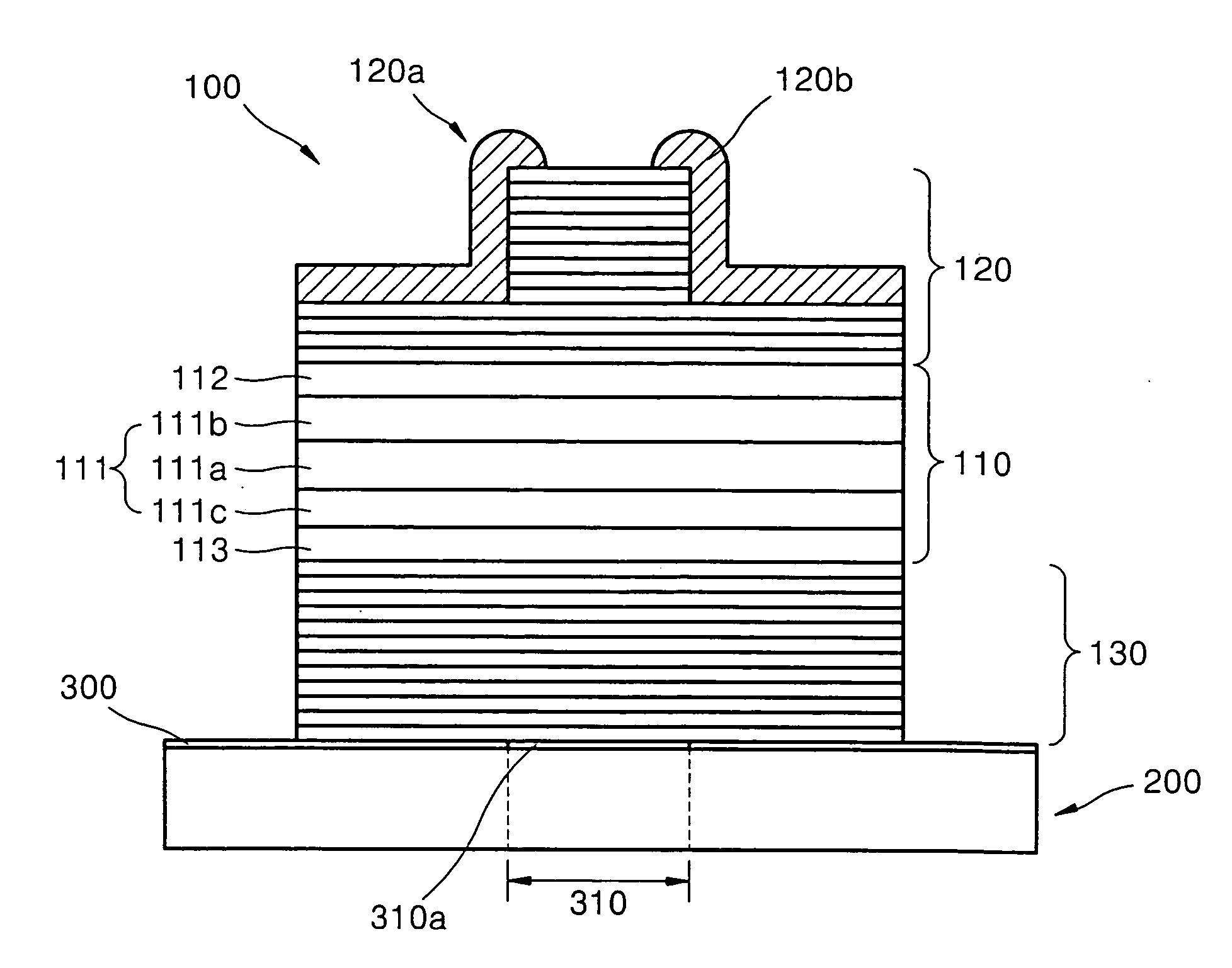
[0021]FIG. 3 schematically illustrates a vertical cavity surface emitting laser (VCSEL) in which a ridge is formed on an upper semiconductor layer. The VCSEL is a well-known lasing structure which includes an active region where lasing occurs and upper and lower semiconductor layers between which the active region is sandwiched. Hence, the following detailed description of the lasing structure does not limit the technical scope of the present invention.

[0022] As shown in FIG. 3, a lasing structure 100 includes an active region 110, which is a cavity where laser resonance occurs, and upper and lower semiconductor layers 120 and 130 of distributed Bragg reflectors (DBR), between which the active region 110 is sandwiched. The lower semiconductor layer 130 includes a substrate (not shown). The active region 110 includes an active layer 111 and cladding layers 112 and 113 between which the active layer 111 is sandwiched. The active layer 111 includes a quantum well layer 111a and barrie...


PUM


Abstract

A vertical cavity surface emitting laser (VCSEL) integrated with a photodetector is provided. The photodetector is attached to a bottom surface of the VCSEL by a bonding layer, which includes a window of a predetermined diameter. The bonding layer is a eutectic bonding layer. An air gap exists within the window and mainly transmits a laser beam. Most of spontaneous emission light incident at an angle is blocked by an area of the bonding layer other than the window, and even some of the spontaneous emission light that heads toward the window cannot easily passes through the window due to a big difference between refractive indices of a semiconductor layer and the air. Thus, the eutectic bonding layer greatly reduces a voltage drop at an interface between the VCSEL and the photodetector, thereby contributing to mass production.

Description

BACKGROUND OF THE INVENTION [0001] This application claims the priority of Korean Patent Application No. 2003-57284, filed on Aug. 19, 2003, in the Korean Intellectual Property Office, the disclosure of which is incorporated herein in its entirety by reference. [0002] 1. Field of the Invention [0003] The present invention relates to a long wavelength vertical cavity surface emitting laser (VCSEL) with an integrated photodetector. [0004] 2. Description of the Related Art [0005] Generally, a VCSEL diode is combined with a photodetector for power monitoring and automatic power control (APC) based on the power monitoring. For example, in U.S. Pat. No. 5,943,357, a photodetector is attached to a long wavelength VCSEL by wafer fusion. [0006]FIG. 1 is a simplified cross-section of a conventional VCSEL to which a photodetector is fused. Referring to FIG. 1, the conventional VCSEL includes an upper semiconductor layer 12 of distributed Bragg reflectors (DBR), an active region 11, and a lower...

Claims


Application Information

Patent Timeline
IPC IPC(8): G11B7/125H01L31/147H01S5/02H01S5/026H01S5/0683H01S5/183
CPCB82Y10/00B82Y20/00H01L31/147H01S5/18377H01S5/0683H01S5/18308H01S5/18375H01S5/0264H01S5/183
Inventor KIM, TAEK
Owner SAMSUNG ELECTRONICS CO LTD
Why Eureka
Try Eureka