Programmable jitter generator

Active Publication Date: 2005-02-24
CREDENCE SYSTEMS
View PDF12 Cites 46 Cited by
  • Summary
  • Abstract
  • Description
  • Claims
  • Application Information

AI Technical Summary

Benefits of technology

The input capacitance of a set of load gates suitably provides the variable capacitance at the buffer outputs. Due to the well-known Miller effect, the input capacitance of a load gate increases when the load gate receives a bias current and decreases when the bias current is turned off. Therefore, in the preferred embodiment of the invention, all load gate inputs are directly connected to the buffer outputs and are connected to a bias voltage though switches controlled by the delay control data. In an alternative embodiment of the invention, a set of switches selectively couple

Problems solved by technology

While a transmitter may synchronize edges in a data signal to edges of a clock signal, a data signal can often appear somewhat jittery to a receiver.
Noise in the signal path conveying the data signal to the receiver can introduce jitter into the data signal.
In a system where the transmitter sends a sampling clock signal to the receiver, noise in the clock signal path can cause the receiver to perceive the data signal to be jittery relative to the clock signal.
In a receiver employing a clock recovery system to generate a local sampling clock signal, feedback errors or noise in the clock recovery system can cause jitter in the sampling clock signal, thereby causing the data signal to appear jittery relative to the sampling clock signal.
A receiver can tolerate some amount of jitter in a digital signal, but when a digital signal is too jittery, the receiver will not be able to correctly determine each successive state of the digital signal from the samples it acquires.
But for high frequency test signals, a typical IC tester may not have sufficient timing resolution to do that.
Even when an IC tester can generate a test signal having a controlled amount of amount of jitter, the signal path between the tester and the IC may be subject to noise.
Thus when the test signal arrives at the IC, it may not only exhibit the controlled amount of jitter introduced by the IC tester, it may also exhibit an

Method used


Image

  • Programmable jitter generator
  • Programmable jitter generator
  • Programmable jitter generator

Examples


Embodiment Construction

The invention relates to a jitter generator for generating a jittery clock or data signal for use in testing an integrated circuit (IC). While this specification illustrates principles of the invention by describing examples considered best modes of practicing the invention, the invention as defined by the claim(s) appended to this specification is not necessarily limited to the particular examples described in the specification below or to the manner in which they operate.

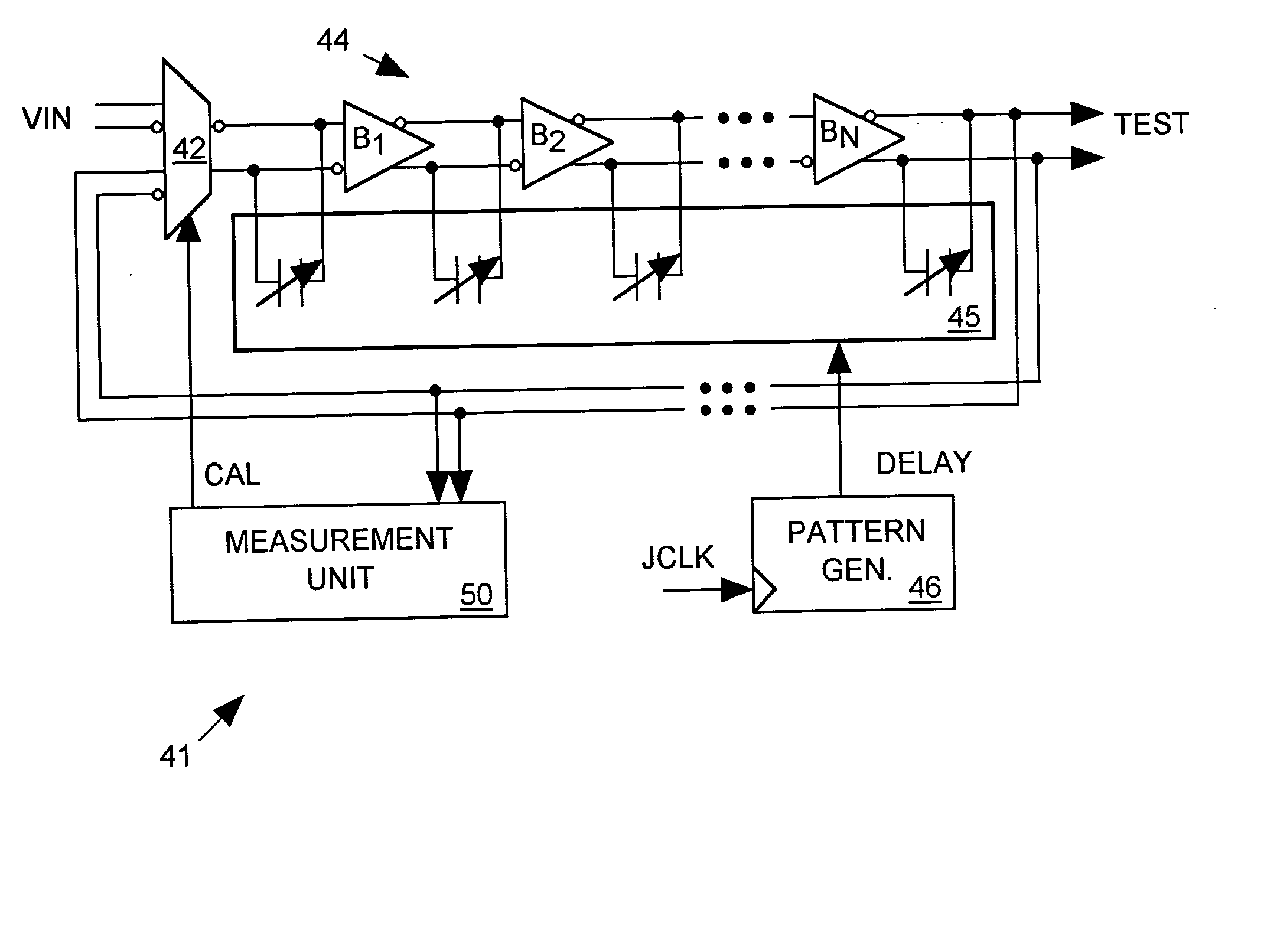
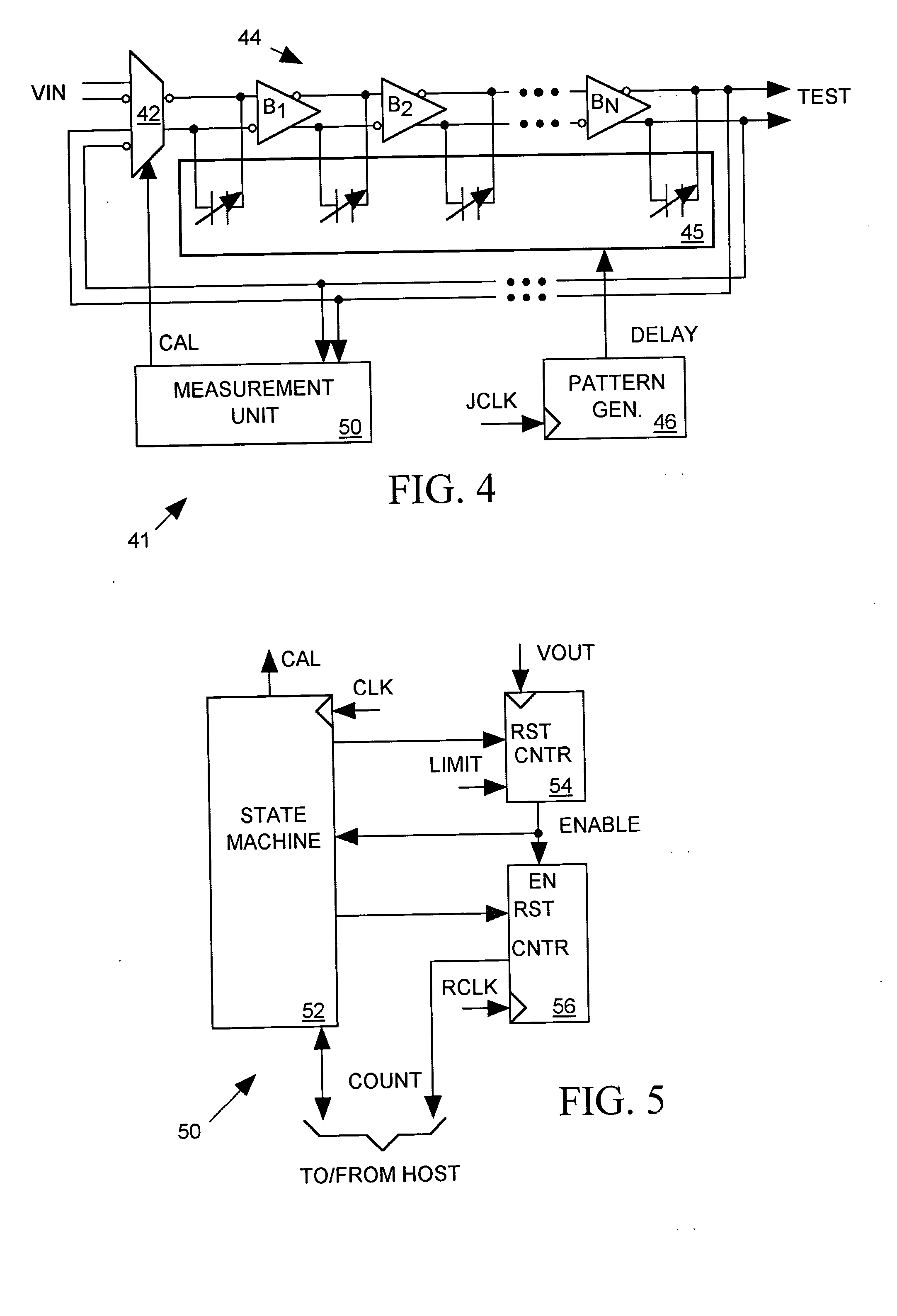
FIG. 4 illustrates an exemplary embodiment of a programmable “jitter generator”41 in accordance with the invention for adding a controlled amount of jitter to an input signal VIN to produce a jittery test signal (TEST). For example when the VIN signal is a clock signal having periodic rising and falling edges, the TEST signal will be a jittery clock signal having the same average period as the VIN signal, but the timing of rising and falling edges of the TEST signal will vary in a controlled manner relative to c...


PUM


Abstract

A jitter generator produces a jittery test signal for use in performing a jitter test on an integrated circuit (IC) device under test (DUT). The jitter generator includes a programmable delay circuit for delaying a non-jittery input signal with a varying delay controlled by input digital delay control data to produce the test signal. A pattern generator supplies a sequence of delay control data to the programmable delay circuit causing it to produce a desired jitter pattern in the test signal. During a calibration process, a measurement unit feeds the test signal back to the input of the programmable delay circuit, causing the test signal to oscillate with a period proportional to the delay through the delay circuit. The measurement unit then measures the period of the test signal for various values of delay control data and reports measurement results. Based on the measurement results, host equipment then determines an appropriate sequence of delay control data for producing a desired jitter pattern in the test signal and programs the pattern generator to produce that sequence of delay control data during a jitter test. The jitter generator can form a part of a built-in, self-test (BIST) circuit implemented within the DUT itself.

Description

BACKGROUND OF THE INVENTION 1. Field of the Invention The invention relates in general to integrated jitter generators for adding a controlled amount of jitter to a signal during a jitter test. 2. Description of Related Art When a transmitting IC transmits a digital data signal to a receiving IC, the transmitter typically synchronizes state changes in the digital data signal to leading (or trailing) edges of a periodic clock signal so that the state changes within the data signal will occur at predictable times. To produce a data sequence represented by successive states of the digital signal, the receiver need only digitize the data signal with an appropriate sampling phase and frequency. In some communication systems, a transmitter sending a digital data signal to a receiver also sends a clock signal to the receiver for controlling the timing with which the receiver samples the data signal. In other communication systems the receiver may include a “clock recovery” system for g...

Claims


Application Information

Patent Timeline
IPC IPC(8): G01R29/26G01R31/28G01R31/317G01R31/3185G01R31/319H03K5/00H03K5/13
CPCG01R29/26G01R31/2841G01R31/31709G01R31/31715H03K5/133G01R31/3191G01R31/31922H03K2005/00026H03K2005/00208G01R31/318533
Inventor FRISCH, ARNOLD M.
Owner CREDENCE SYSTEMS
Why Eureka
Try Eureka