

Ultra high-speed si/sige modulation-doped field effect transistors on ultra thin soi/sgoi substrate
a field effect transistor and modulation-doped field effect technology, which is applied in the direction of semiconductor devices, semiconductor/solid-state device details, electrical apparatus, etc., can solve the problems of reducing self-heating and driving current, and achieve high rf performance
- Summary
- Abstract
- Description
- Claims
- Application Information
AI Technical Summary
Benefits of technology
Problems solved by technology
Method used
Image

Examples
first embodiment
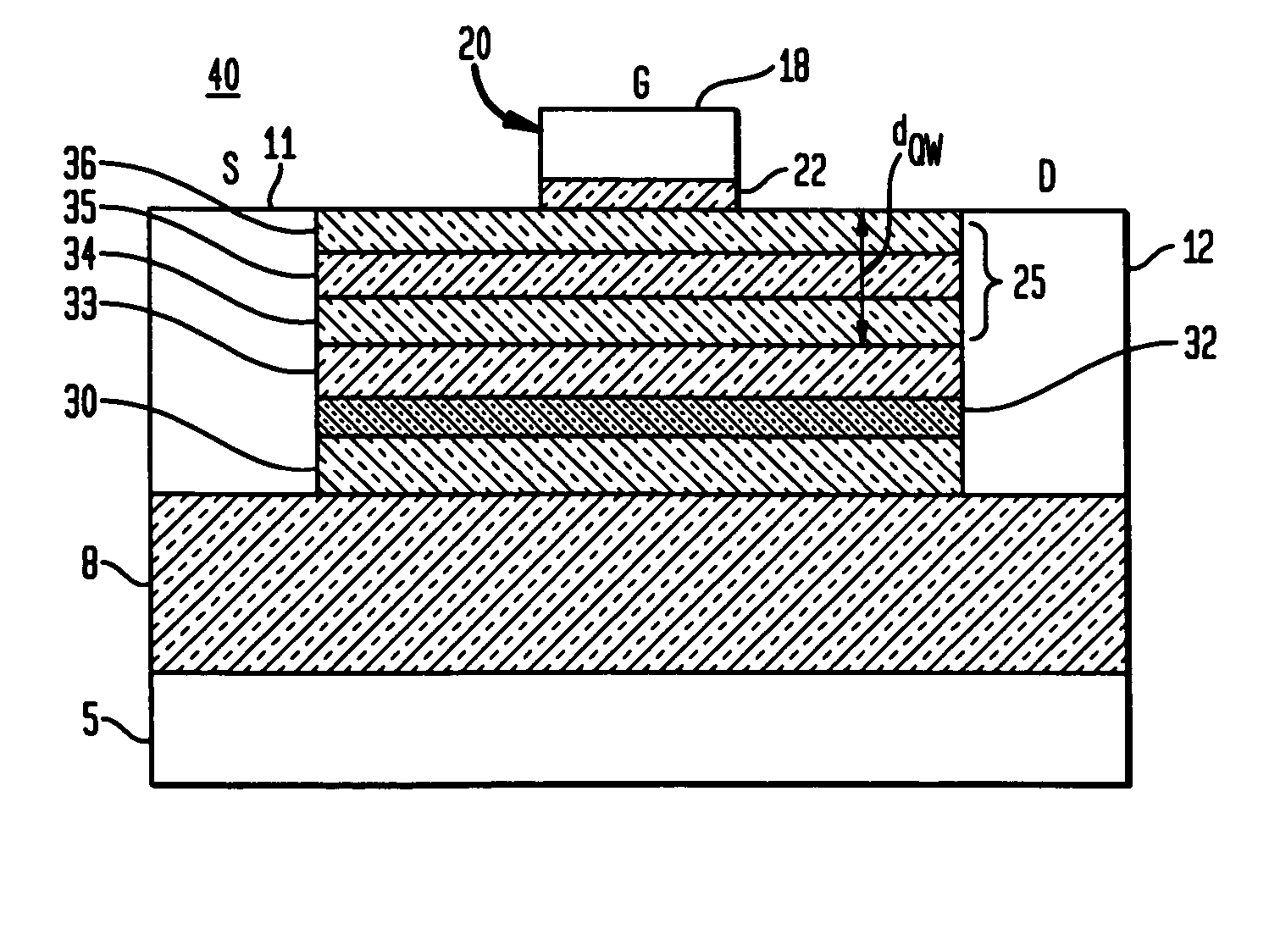
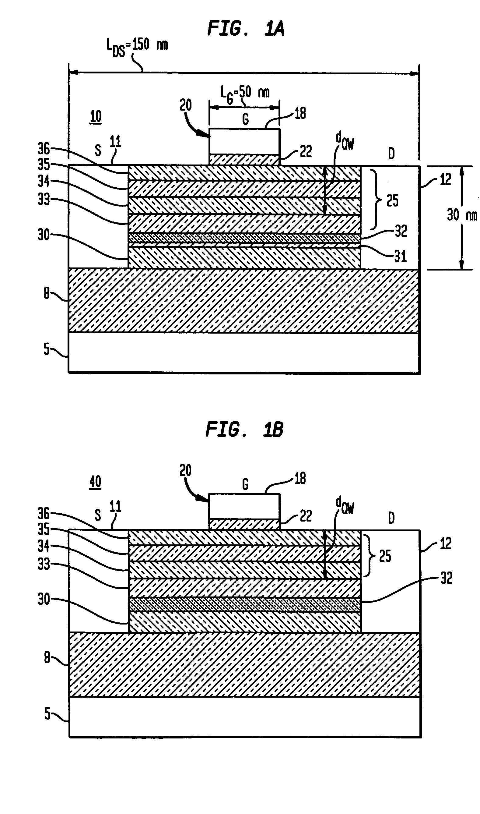
[0033]FIG. 1(a) particularly depicts a MODFET device according to a As shown in FIG. 1(a), there is depicted a top doped nMODFET device 10 comprising a Si substrate layer 5, a buried dielectric layer 8 formed on top of the substrate 5 which may range up to 200 nm in thickness and comprise an oxide, nitride, oxynitride of silicon; and a channel region 25 formed between n+-type doped source and drain regions 11, 12 respectively, and a gate structure 20 including a gate dielectric layer 22 separating the gate conductor 18 from the channel 25. As shown in the figure, the gate dielectric layer may comprise an oxide, nitride, oxynitride of silicon, and oxides and silicates of Hf, Al, Zr, La, Y, Ta, singly or in combinations. It is important to realize that according to the invention, the dimensions of the device including drain, source, gate and channel regions have been scaled.
[0034] The composition of the channel region 25 of device 10 in FIG. 1(a) is as follows: A relaxed SiGe layer 3...
fifth embodiment
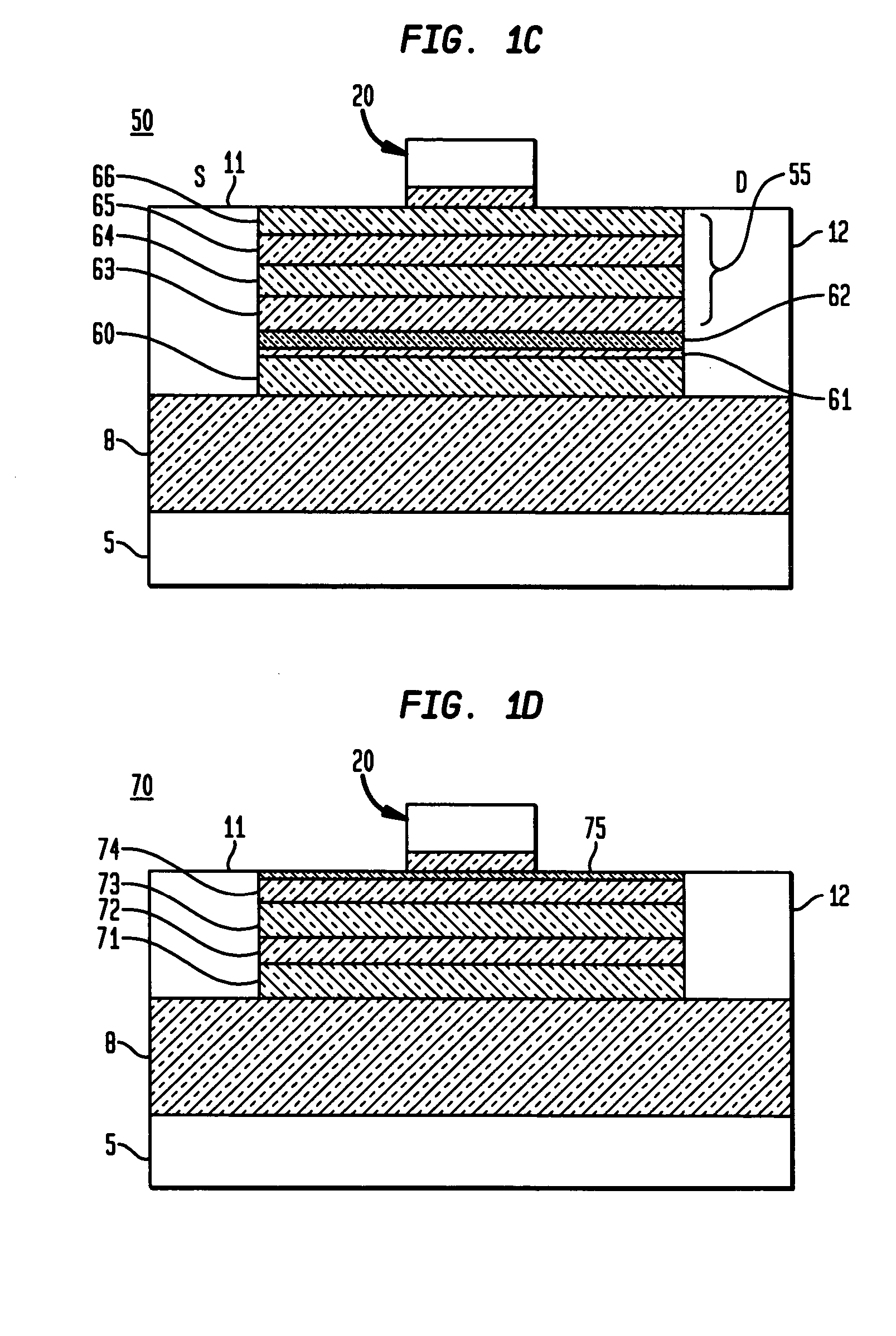
[0040]FIG. 1(f) illustrates the invention drawn to a high-hole-mobility MODFET device 80 that is bottom doped and including a doped transferred layer. As shown in FIG. 1(f), the pMODFET device 90 includes an SGOI (SiGe layer 91 on insulator 8) substrate having: a relaxed epitaxial Si1−jGej supply layer ranging in thickness between 5 nm-25 nm, and having ion-implanted or in-situ p-type doping of a concentration ranging between 1e18-5e19 cm−3 and serving as a supply layer. Alternately, the relaxed Si1−jGej layer may be predoped p-type to a concentration level of 1e18-5e19 boron atoms / cm3 before a layer transfer in forming the SGOI substrate; an epitaxial Si1−kGek spacer layer 92 grown on top of the supply layer 91 and ranging in thickness between 3 nm-7 nm; an epitaxial compressively strained Si1−mGem channel layer 93 grown on top of the spacer layer and ranging in thickness between 5 nm-20 nm; and, an epitaxial strained Si1−nGen cap layer 94 grown on top of the strained Si1−mGem chan...
PUM
 Abstract
Description
Claims
Application Information