Method and system for providing a magnetic element including passivation structures
- Summary
- Abstract
- Description
- Claims
- Application Information
AI Technical Summary
Benefits of technology
Problems solved by technology
Method used
Image

Examples
first embodiment
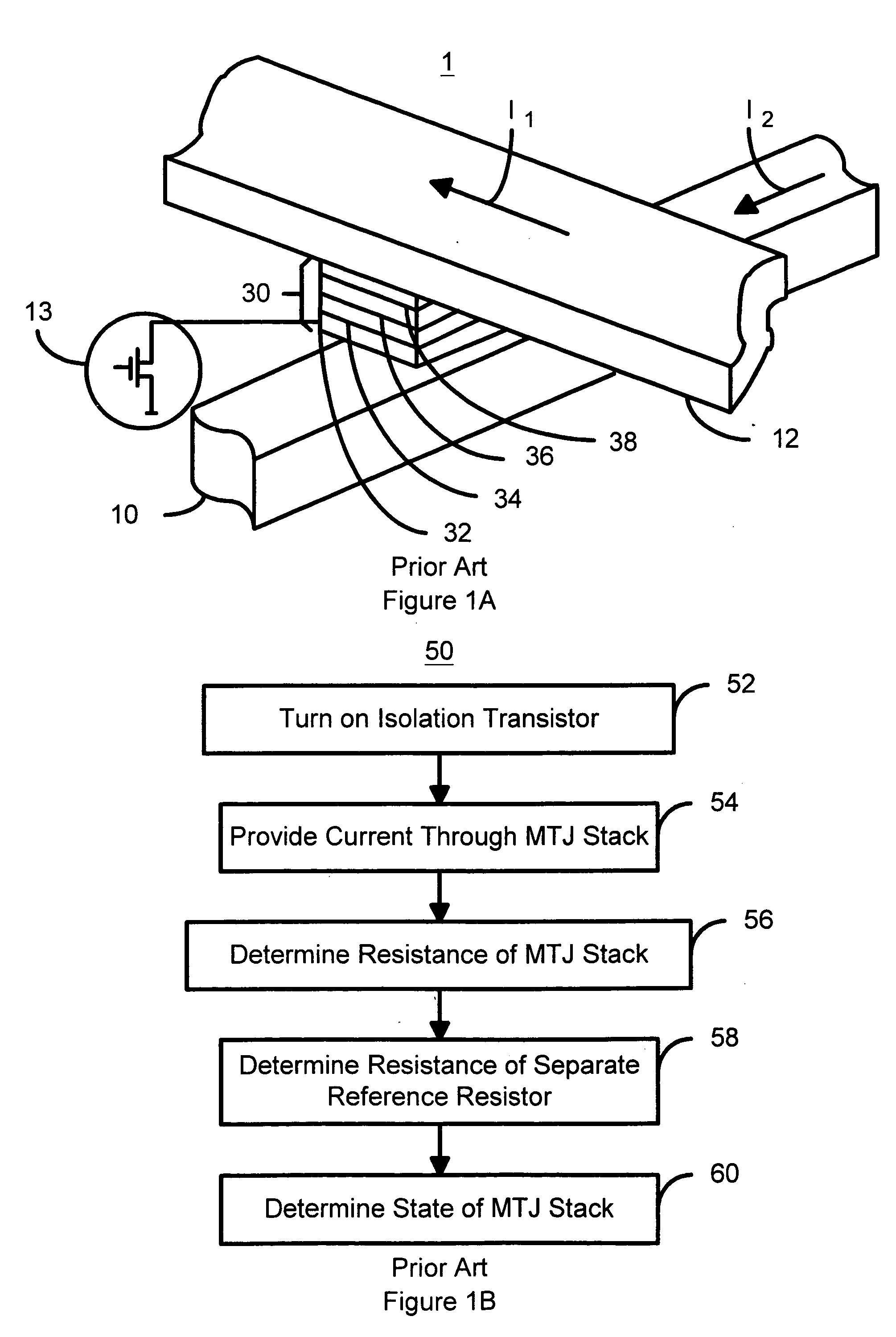
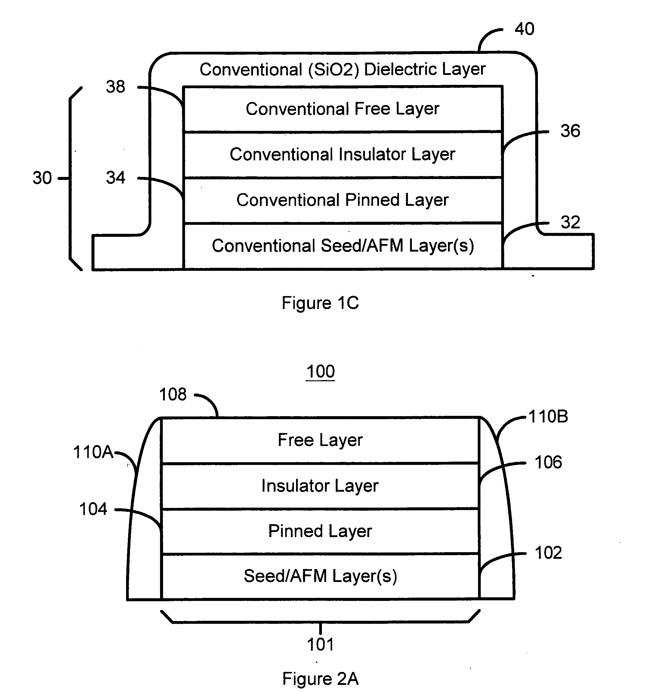
To more particularly illustrate the method and system in accordance with the present invention, refer now to FIG. 2A depicting a magnetic element 100 in accordance with the present invention. The magnetic element 100 includes passivation layers 110A and 110B as well as storage portion that is preferably a MTJ stack including at least layers 102, a pinned layer 104, an insulator layer 106, and a free layer 108. However, another type of magnetic element could be used. The layers 102 preferably include at least one seed layer and an AFM layer used to pin the magnetization of the pinned layer 104. The insulator layer 106 is a tunneling barrier between the pinned layer 104 and the free layer 108 and is preferably Al2O3. The magnetization of the free layer 108 rotates in response to an external magnetic field and thus is used to store data. Based upon the orientations of the magnetizations of the free layer 108 and pinned layer 104 (antiparallel or parallel), the resistance of the magneti...
second embodiment
FIG. 2B depicts a magnetic element 120 in accordance with the present invention. The magnetic element 120 includes an MTJ stack 121 including layers 122, 124, 126, and 128. The MTJ stack 121 is analogous to the MTJ stack 101 depicted in FIG. 2A and will, therefore, not be further described. Referring to FIGS. 2A and 2B, the magnetic element 120 also includes a passivation layer 130A and 130B. The passivation layer 130A and 130B covers the sides and a portion of the top of the MTJ stack 121. In addition, the passivation layer 130A and 130B covers the surfaces between MTJ stacks 121. Thus, the only apertures opened in the passivation layer 130A and 130B are preferably those above the MTJ stack 121. The materials used for and processes used in forming the materials for the passivation layer 130A and 130B are substantially the same as for the passivation layer 110. For example, Si3N4, SizNyHz, AlN, Ta2O5 and the same material as the insulator layer 126 could be used for the passivation ...
third embodiment
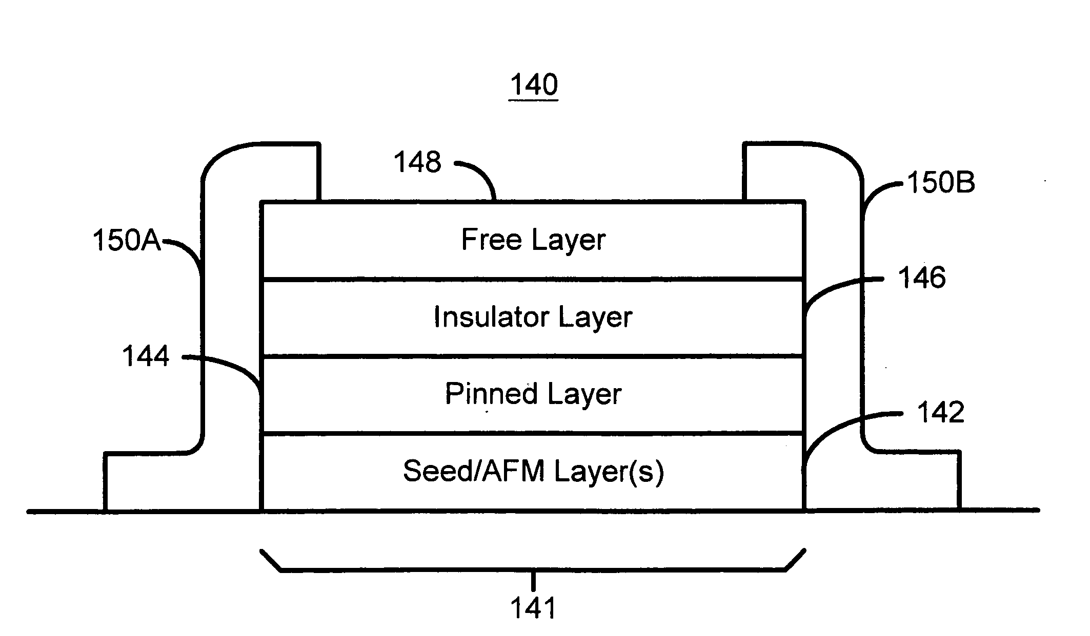
FIG. 2C depicts a magnetic element 140 in accordance with the present invention. The magnetic element 140 includes an MTJ stack 141 including layers 142, 144, 146, and 148. The MTJ stack 141 is analogous to the MTJ stack 101 depicted in FIG. 2A and will, therefore, not be further described. Referring to FIGS. 2A and 2C, the magnetic element 140 also includes a passivation layer 150A and 150B. The passivation layer 150A and 150B covers the sides and a portion of the top of the MTJ stack 141. The materials used for and processes used in forming the materials for the passivation layer 150A and 150B are substantially the same as for the passivation layer 110. For example, Si3N4, SizNyHz, AlN, Ta2O5 and the same material as the insulator layer 146 could be used for the passivation layer 150A and 150B.
The passivation layer 150A and 150B covers the sides and a portion of the top of the MTJ stack 141, rather than covering only the sides of the MTJ stack as for the passivation layer 110. In...
PUM
 Abstract
Description
Claims
Application Information