Method for fabricating electronic device

a technology of electronic devices and wire forming, which is applied in the direction of semiconductor devices, semiconductor/solid-state device details, electrical devices, etc., can solve the problems of voids created in the lower layer wiring, metal film has a discontinuous portion, and the interlayer insulating film cannot be guaranteed, so as to prevent the increase of low dielectric constant film and reduce the wiring capacitance

Active Publication Date: 2005-03-03
PANNOVA SEMIC
View PDF2 Cites 45 Cited by
  • Summary
  • Abstract
  • Description
  • Claims
  • Application Information

AI Technical Summary

Benefits of technology

[0052] In this case, wiring capacitance can be reduced. Moreover, since the first barrier metal film is formed on the side walls of the hole, the second insulating film is not damaged by the process using a reducing gas. Therefore, the dielectric constant of the low dielectric constant film can be prevented from increasing.

Problems solved by technology

The deposit of copper moves into the interlayer insulating film in a following process such as a heating process, so that it causes a problem such as a leak between wirings.
Simultaneously, the copper of the lower layer wiring is diffused into the interlayer insulating film by using the deposit as a diffusion path, so that a problem such stress migration that a void is created in the lower layer wiring occurs.
When the thickness of the barrier metal film formed on the side wall of the interlayer insulating film decreases as a semiconductor integrated circuit is becoming finer, sufficient thickness of the barrier metal film formed on the deposit of copper on the side wall of the interlayer insulating film cannot be assured and, moreover, the barrier metal film comes to have a discontinuous portion.
Consequently, an interface state of excellent adhesion between the barrier metal film and the copper film formed on the barrier metal film cannot be assured and a nucleus formation site of a void is generated in the interface between the barrier metal film and the copper film.
It causes poor reliability of a semiconductor integrated circuit, particularly, a problem such as electro-migration or stress migration.
When the barrier metal film has a thin portion or a discontinuous portion, a failure may occur after formation of the wiring.
Concretely, a failure occurs due to heat generated in a heat treatment process in the upper layer wiring forming process performed after formation of the barrier metal film or heat generated at the time of a high-temperature storage test after completion of the device.
As a result, a failure related to stress migration such as generation of a leak current to the interlayer insulating film and formation of a void in the copper film of the connection hole occurs.

Method used


Image

  • Method for fabricating electronic device
  • Method for fabricating electronic device
  • Method for fabricating electronic device

Examples


embodiment 1

[0062] Embodiment 1

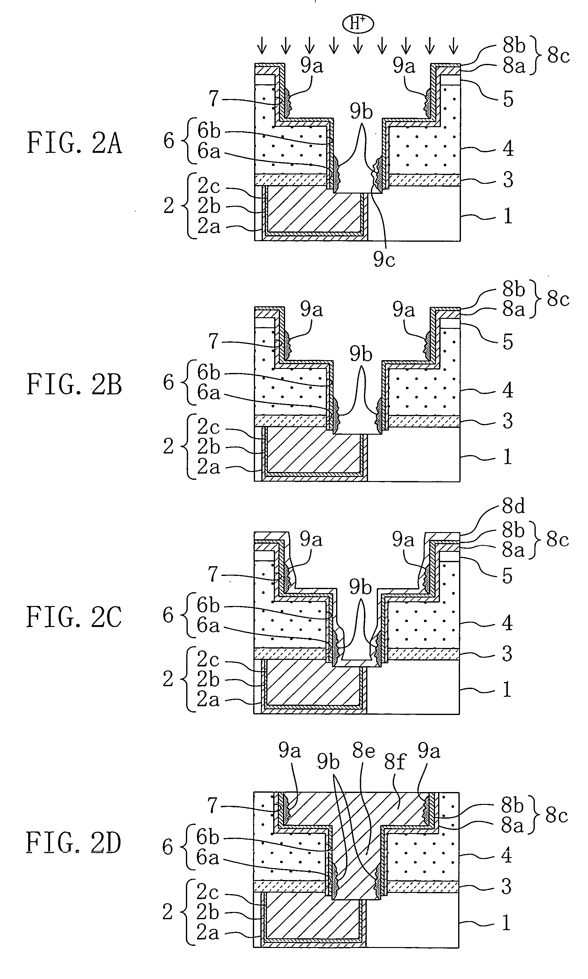
[0063] A method for fabricating an electronic device according to a first embodiment of the invention will be described with reference to FIGS. 1A to 1D and FIGS. 2A to 2D.

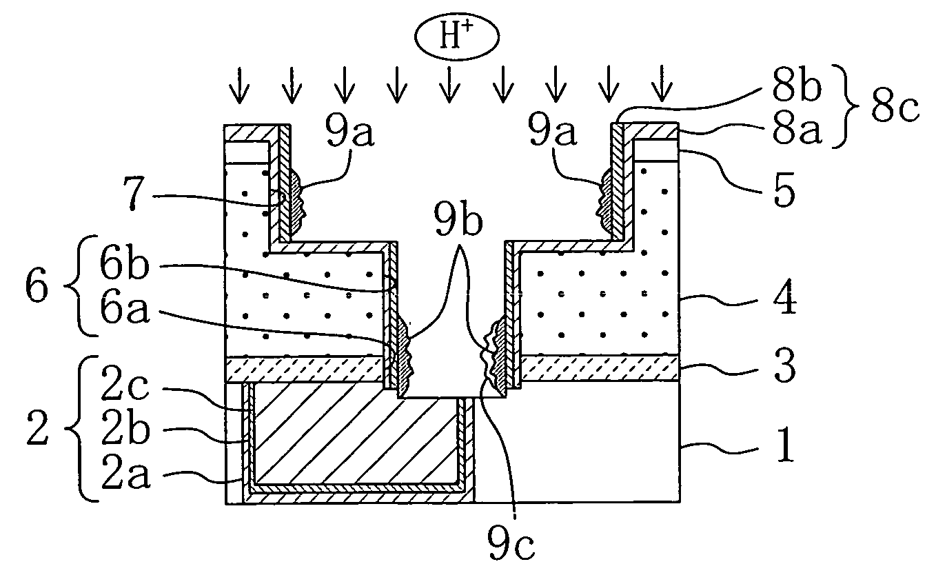
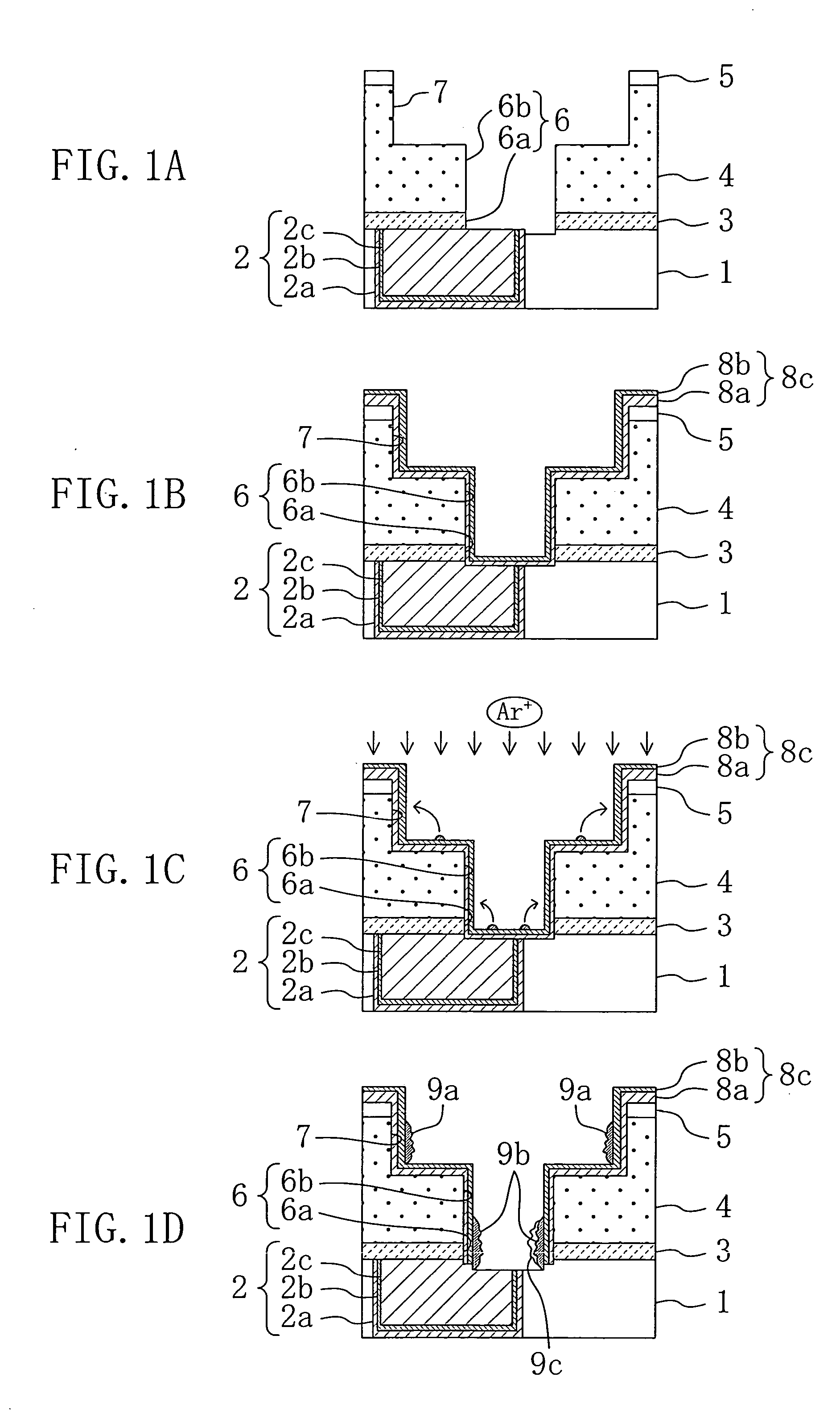
[0064]FIGS. 1A to 1D and FIGS. 2A to 2D are cross sections each showing a state where an electronic device is designed without an alignment margin between a connection hole and a wiring formed in a lower layer, and the connection hole is deviated from the wiring formed in the lower layer due to misalignment or dimensional variations which occur at the time of lithography for forming the connection hole or dimensional variations which occur at the time of dry etching.

[0065] As shown in FIG. 1A, first, a first wiring trench pattern is formed by photolithography in a first insulating film 1 made of a silicon oxide film formed on a silicon substrate (not shown), and dry etching is performed on the first insulating film 1, thereby forming a first wiring trench having a depth of 250 nm in the first ...

embodiment 2

[0096] Embodiment 2

[0097] A method for fabricating an electronic device according to a second embodiment of the invention will now be described with reference to FIGS. 3A to 3C and FIGS. 4A to 4C.

[0098] First, in the second embodiment, the processes shown in FIGS. 1A and 1B in the first embodiment are performed in a manner similar to the first embodiment.

[0099] Next, by performing sputter etching using argon gas as shown in FIG. 3A, the tantalum nitride film 8a and the tantalum film 8b exposed from the bottom of the connection hole 6 are removed and a natural oxide film existing on the interface with the first barrier metal film 8c is removed.

[0100] The sputter etching using argon gas is performed so that the first barrier metal film 8c formed on the bottom of the second wiring trench 7 and the surface of the third insulating film 5 exist as shown in FIG. 3B which will be described later. Alternately, etching may be performed so that the tantalum film 8b remains in a manner simil...


PUM


Abstract

A method for fabricating an electronic device includes: a step of forming a first conductor to become a wiring or a wiring plug in a first insulating film; a step of forming a second insulating film on the first insulating film and the first conductor and, after that, forming a hole reaching the top face of the first conductor in the second insulating film; a step of forming a first barrier metal film on a bottom and side walls of the hole and on the second insulating film; a step of removing a portion formed on the bottom of the hole in the first barrier metal film to thereby expose the top face of the first conductor; a step of performing a plasma process using a reducing gas after the step of exposing the top face of the first conductor; and a step of forming a second conductor to become a wiring plug or a wiring by filling a conductive film in the hole after the step of performing the plasma process.

Description

CROSS-REFERENCE TO RELATED APPLICATION [0001] All of the matters disclosed in the specification, drawings, and claims of Japanese Patent Laid-open No. 2003-301927 filed on Aug. 26, 2003 are incorporated by reference herein. BACKGROUND OF THE INVENTION [0002] The present invention relates to a method for fabricating an electronic device and, more particularly, to a wiring forming technique. [0003] In recent years, reduction in size, higher packing density, and higher speed of a semiconductor integrated circuit are in demand and, accordingly, reduction in wiring resistance and wiring capacitance and improvement in reliability of a semiconductor integrated circuit are necessary. To realize reduction in wiring resistance and improvement in reliability of a semiconductor integrated circuit, copper wiring having specific resistance lower than that of a conventional aluminum alloy and having high reliability is used in practice. [0004] To reduce wiring capacitance, an insulating film havin...

Claims


Application Information

Patent Timeline
Patent Type & Authority Applications(United States)
IPC IPC(8): H01L21/3205H01L21/768H01L21/3065H01L23/52
CPCH01L21/76805H01L21/76861H01L21/76846H01L21/76844
Inventor MATSUMOTO, SUSUMU
Owner PANNOVA SEMIC
Why Eureka
Try Eureka