Detector for electromagnetic radiation assisted by majority current

a technology of electromagnetic radiation and detector, applied in the field of electromagnetic radiation detection, can solve the problem that the proportion of minority carriers that reach effectively the target accumulation zone is far from optimal, and achieve the effect of reducing the capacitance of the detection region, fast and sensitive detector, and reducing the capacitan

Active Publication Date: 2005-03-10
SOFTKINETIC SENSORS
View PDF4 Cites 47 Cited by
  • Summary
  • Abstract
  • Description
  • Claims
  • Application Information

AI Technical Summary

Benefits of technology

[0005] The present invention aims to provide a novel photo-detector structure that has a detection region, e.g. a diode junction such as a pn-junction (semiconductor-semiconductor) detection area or a Schottky junction (metal-semiconductor) detection area that can be of an order of magnitude smaller in area than the effective light sensitive area thereby lowering considerably the capacitance of the detection region, e.g. detecting diode-junction. Further, it is also an aim of the invention to provide a method of collecting photo-generated carriers that are present deeply in the substrate, in a fast way, in order to obtain a fast and sensitive detector.

Problems solved by technology

There are however two major deficiencies with these photonic mixers.
Firstly, for light that is absorbed more deeply in the substrate, the generated minority carriers will have to diffuse towards the surface before the modulation photo-gates can redirect these carriers towards the destination accumulation zones.
Second, the percentage of detected minority carriers that reach effectively the target accumulation zone is far from optimal.

Method used


Image

  • Detector for electromagnetic radiation assisted by majority current
  • Detector for electromagnetic radiation assisted by majority current
  • Detector for electromagnetic radiation assisted by majority current

Examples


first embodiment

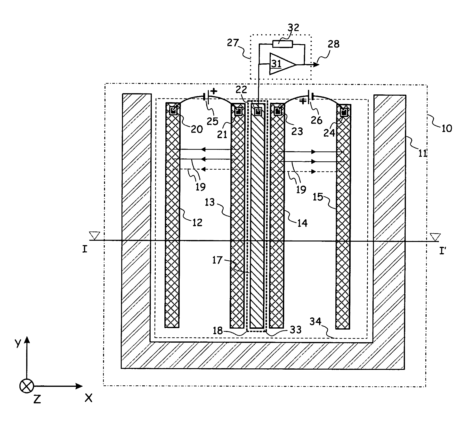
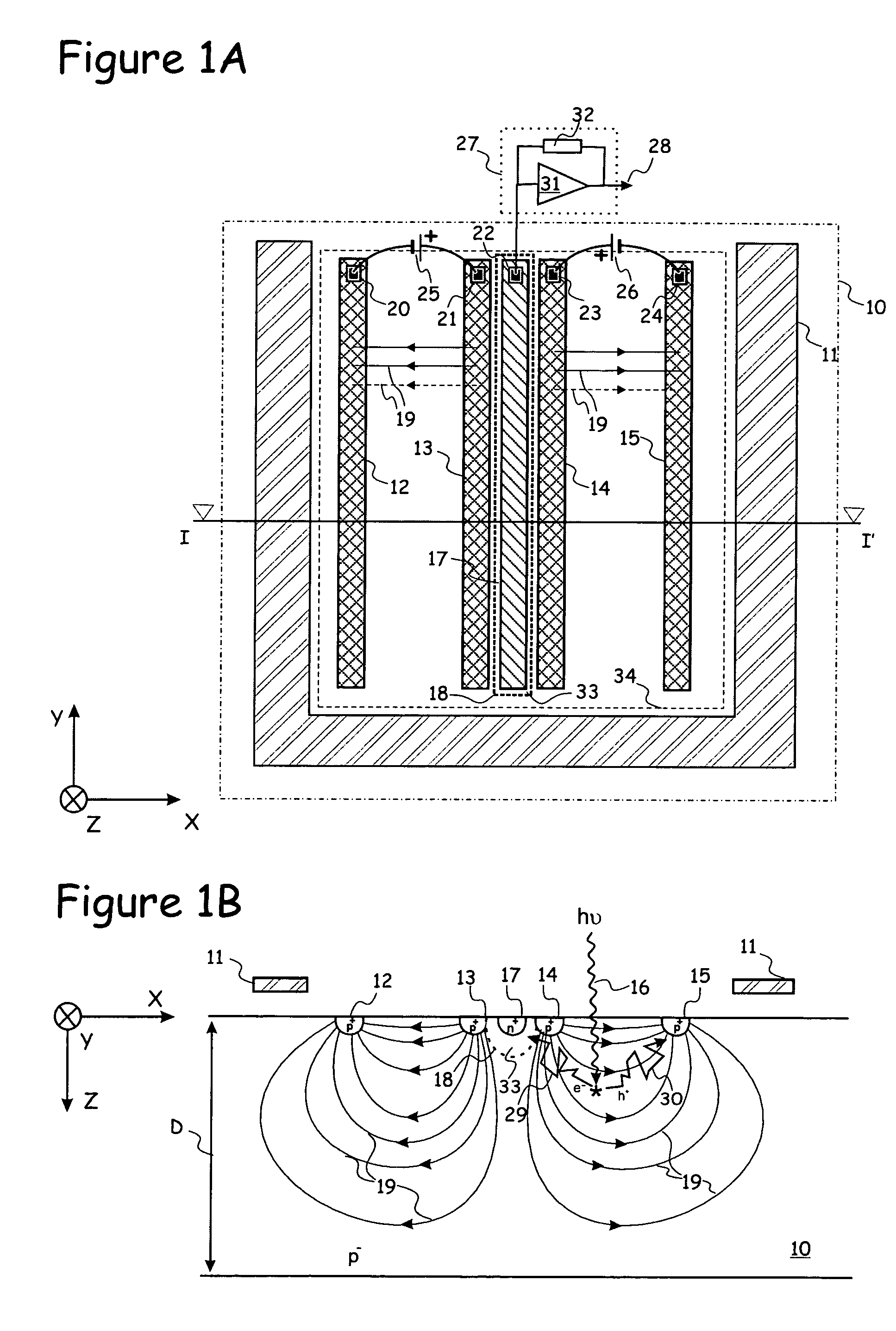
[0040]FIG. 1A shows a top view of a photo-detector according to the present invention. Sources 25 and 26 inject current at contacts 21 and 23 respectively, and drain current at contacts 20 and 24 respectively. Contacts 20, 21, 23 and 24 connect through ohmic-conduction to highly doped regions having a first conductivity type, e.g. p+-regions 12, 13, 14 and 15 respectively. In a resistive, lightly doped substrate having the first conductivity type, e.g. p− substrate 10, a majority carrier current, in the case of a substrate being a p− substrate, a hole current 19 will flow from region 13 to region 12, and from region 14 to region 15. Line I-I′ in FIG. 1A shows where the cross-section is made for FIG. 1B. In FIG. 1B, the majority hole current 19 is shown by solid lines whereby the direction of the hole current 19 is indicated by arrows. In the substrate 10, where the doping is typically considered to be constant, the majority current 19 is associated with an electrical field, in the d...

second embodiment

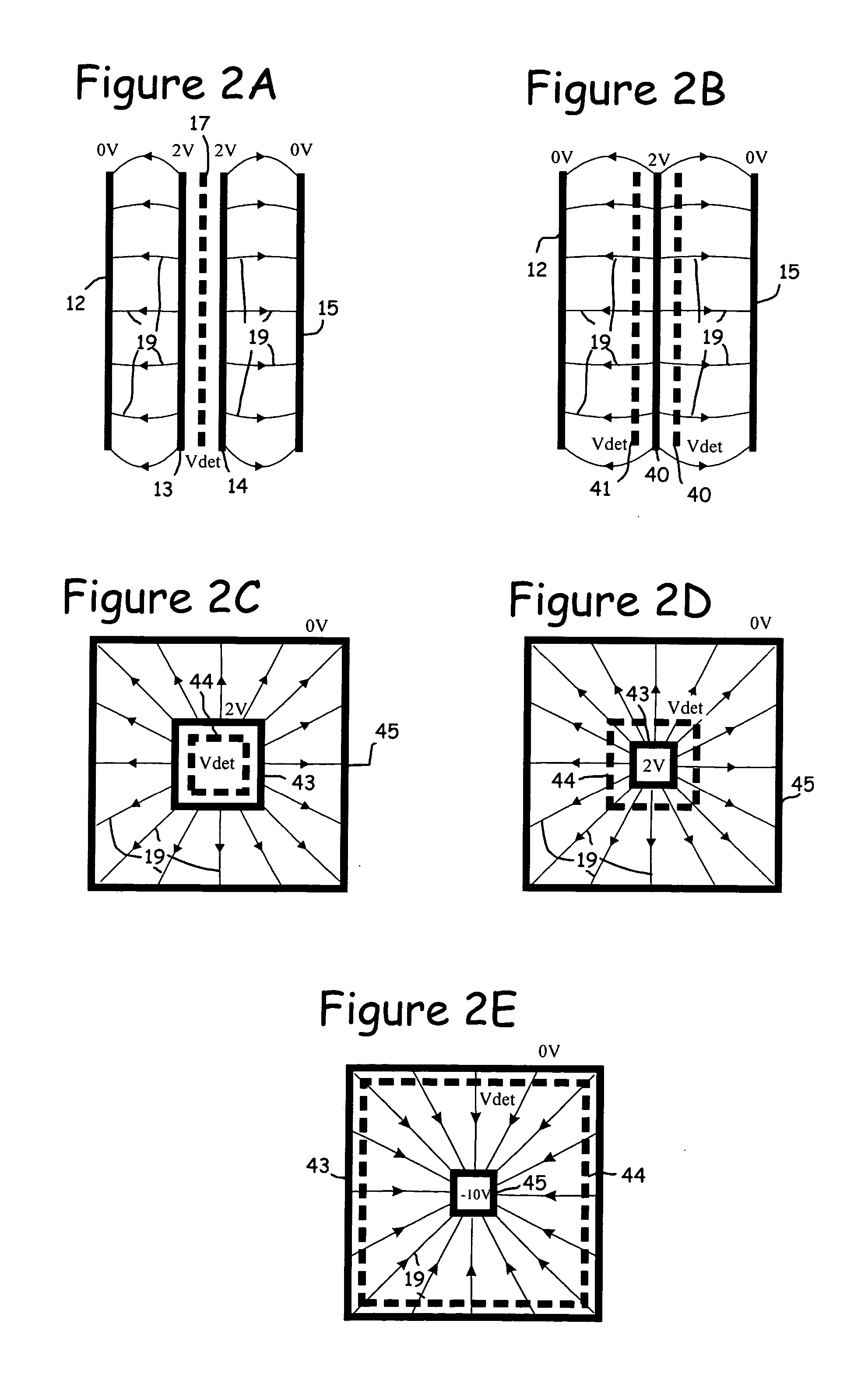
[0051]FIG. 2B shows a detector according to the present invention. It comprises only one source region 40 for injection of the majority current 19, with at each side of it a detector finger 41, 42. In the embodiment shown, the source region 40 is located in the middle of the device. The detector fingers 41, 42 should be connected in parallel. This set-up enhances the speed of the diffusion part of the detecting process, but it also doubles the detector capacitance, since the number of detector fingers 41, 42 is doubled.

[0052]FIGS. 2C and 2D illustrate detectors of a rectangular type.

[0053] Especially the embodiment of FIG. 2C is considered a preferred arrangement or best mode example, since in this embodiment the detector capacitance becomes extremely low. Instead of using a detector finger 17, which for example has a dimension of 40 μm×3 μm, there is a detecting pn-junction 44 with an area that can be as small as of the order of only 3 μm×3 μm, whilst the sensitive light input are...

third embodiment

[0054] The detector of the third embodiment illustrated in FIG. 2D has in the centre its current source region 43, surrounded by a detecting pn-junction 44. Here the detector capacitance is somewhat higher, since the area of the detecting pn-junction 44 is somewhat larger, but it remains low. This set-up enhances the speed of the diffusion part of the detecting process, since the current source region 43 is surrounded by the detecting pn-junction 44.


PUM


Abstract

The present invention relates to a novel photo-detector structure and method whereby light is detected in a semiconductor substrate. Through the use of a small current of majority carriers an electrical field is created that directs photo-generated minority carriers towards a detection region. In this way, a large sensitive area 34 for a detector can be designed with a detection region having low junction area and low associated detector capacitance, thus enhancing output signal to noise ratio and/or speed of attached readout circuits. Simultaneously, the assistant majority current can sweep the minority carriers from deep within the substrate towards the detection region, thus improving the overall detector sensitivity. By making the majority current reconfigurable, a photonic mixer structure with two or more detection regions can be conceived, whereby the direction of the applied current will determine in an efficient way to which detection region the photo-generated minority carriers will be directed. In this way, incident modulated light can get demodulated, such that phase and amplitude of the modulated light can be measured for a.o. range-finding applications.

Description

FIELD OF THE INVENTION [0001] The present invention relates to the field of detection of electromagnetic radiation that generates minority carriers in a semi-conductor substrate, such as for example, but not limited to, detection of visible and infrared light. More particularly, the present invention relates to electromagnetic radiation detection in a substrate and more specifically on the application of a majority current for directing photo-generated minority charges towards a detection region as well as an apparatus therefor. [0002] Technical Background of the Invention [0003] U.S. Pat. No. 6,157,035 describes how a fast detector in a standard CMOS technology can be constructed. A shadow mask gives a spatial modulation to the incident, and consequently of the absorbed light in the semiconductor substrate. By measuring the magnitude of the spatial frequency component in the minority carrier distribution with a spatial frequency corresponding to that of the shadow mask, a fast dete...

Claims


Application Information

Patent Timeline
Patent Type & Authority Applications(United States)
IPC IPC(8): G01J1/42G01T1/24H01L31/0352H01L31/101
CPCH01L31/0352G01S7/4913G01S7/4816H01L31/101G01S17/894
Inventor KUIJK, MAARTENNIEUWENHOVE, DANIEL VAN
Owner SOFTKINETIC SENSORS
Why Eureka
Try Eureka