Switching semiconductor device and switching circuit

a switching circuit and semiconductor technology, applied in the field of switching semiconductor devices and switching circuits, can solve the problems of enormous increase in the power of switchable signals, gan-based hfet facing the disadvantage of high on resistance rsub>on/sub>, and achieve the effect of effective transmission, reducing off capacitance coff, and reducing the characteristic of insertion loss

Active Publication Date: 2005-03-10
PANASONIC CORP
View PDF10 Cites 25 Cited by
  • Summary
  • Abstract
  • Description
  • Claims
  • Application Information

AI Technical Summary

Benefits of technology

[0011] The HFET consisting of AlGaN or GaN is quite promising as a device employed in a high-frequency switching circuit for the following reasons. First, a high dielectric breakdown voltage of GaN can tremendously increase a switchable signal power. Normally, a signal power which can pass through the switching circuit is determined by an opposite-direction breakdown voltage and a threshold voltage Vth of the HFET. A breakdown voltage of the GaN-based HFET is several times as high as that of the GaAs-based FET. It is, therefore, possible to switch high power signal.
[0025] It is preferable that in the switching semiconductor device according to the present invention, the gate electrode is composed of a single gate electrode, and that the switching semiconductor device further comprises a booster circuit which applies a boosted voltage, obtained by boosting a power supply voltage, to the gate electrode. By doing so, the number of stages of transistors can be reduced by the booster circuit. Besides, even with the single gate structure having a single gate, the RF signal with high input power can be switched.

Problems solved by technology

However, the AlGaN / GaN HFET has never been employed in a high-frequency switching circuit.
First, a high dielectric breakdown voltage of GaN can tremendously increase a switchable signal power.
Although the GaN-based HFET is quite promising as a high-frequency switching circuit device, the GaN-based HFET confronts the disadvantage of high ON resistance Ron.

Method used


Image

  • Switching semiconductor device and switching circuit
  • Switching semiconductor device and switching circuit
  • Switching semiconductor device and switching circuit

Examples


embodiment 1

[0057] A first embodiment of the present invention will be described with reference to the drawings.

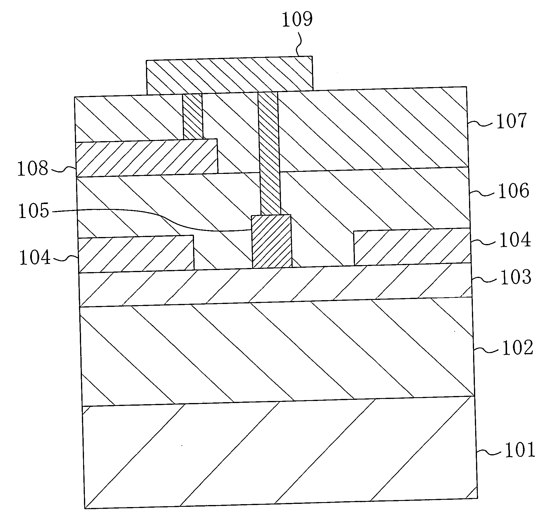
[0058]FIG. 1 depicts a sectional configuration of a switching semiconductor device according to a first embodiment of the present invention. As shown in FIG. 1, a heterojunction field-effect transistor (HFET) which serves as the switching semiconductor device according to the first embodiment includes a first compound layer 102 and a second compound layer 103 which are sequentially formed on a single crystal substrate 101 consisting of high-resistance silicon carbide (SiC) by epitaxial growth. The first compound layer 102 consists of undoped InxGa1-xN (where 0≦x≦1) and has a thickness of about 3 μm, and the second compound layer 103 consists of undoped InyAlzGa1-y-zN (where 0≦y≦1 and 0

[0059] The first compound layer 102 and the second compound layer 103 each having a heterojunction surface form a so-called modulation dope structure in which charges are supplied by a polarizati...

modification 1

OF EMBODIMENT 1

[0069] A first modification of the first embodiment according to the present invention will be described with reference to the drawings.

[0070]FIG. 3 depicts a sectional configuration of a switching semiconductor device according to the first modification of the first embodiment of the present invention. In FIG. 3, the same constituent elements as those shown in FIG. 1 are denoted by the same reference numerals, and will not be described herein.

[0071] As shown in FIG. 3, the switching semiconductor device according to the first modification includes a third compound layer 201 which consists of undoped AluGa1-uN (where 0101 which consists of silicon carbide and a first compound layer 102, and which has a thickness of about 1 μm.

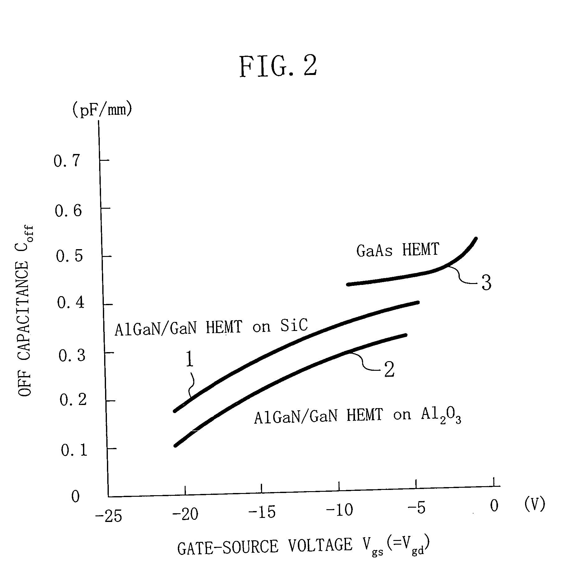
[0072] As already described, AluGa1-uN is lower in dielectric constant than silicon carbide. Therefore, the OFF capacitance Coff of the switching semiconductor device can be further reduced and the isolation characteristic thereof can be furth...

modification 2

OF EMBODIMENT 1

[0075] A second modification of the first embodiment according to the present invention will be described with reference to the drawings.

[0076]FIG. 5 depicts a sectional configuration of a switching semiconductor device according to the second modification of the first embodiment of the present invention. In FIG. 5, the same constituent elements as those shown in FIG. 3 are denoted by the same reference numerals, and will not be described herein.

[0077] As shown in FIG. 5, the second modification differs from the first modification in the following respects. Sapphire is used for a single crystal substrate 301. A gate insulating film 302 which consists of, for example, gallium oxide (Ga2O3) and which has a thickness of about 10 nm is formed between a second compound layer 103 and a gate electrode 105, whereby the switching semiconductor device is formed as a so-called MIS FET (Metal Insulator Semiconductor FET). A material for the gate insulating film 302 is not limit...


PUM


Abstract

A switching semiconductor device includes a first compound layer formed on a single crystal substrate which consists of silicon carbide or sapphire, and consisting of a general formula InxGa1-xN, where 0≦x≦1; a second compound layer formed on the first compound layer, and consisting of a general formula IyAlzGa1-y-zN, where 0≦y≦1 and 0<z≦1; and a gate electrode formed on the second compound layer. The gate electrode is electrically connected to a resistance element formed on a first interlayer insulating film that covers the gate electrode, through a metal wiring formed on a second interlayer insulating film that covers the first interlayer insulating film.

Description

CROSS-REFERENCE [0001] All the matters disclosed in the claims, the specification, and the drawings of Japanese Patent Application No. 2003-296060 filed on Aug. 20, 2003 are incorporated herein by reference. BACKGROUND OF THE INVENTION [0002] The present invention relates to a switching semiconductor device and a switching circuit employed in a radio-frequency communication apparatus such as a cellular telephone. [0003] Recently, a high-frequency switching circuit which switches over a high-frequency signal transmitted or received through an antenna between a transmitter-side circuit and a receiver-side circuit has been widely employed in a mobile communication apparatus represented by a cellular telephone. Important electric characteristics of the high-frequency switching circuit are an insertion loss characteristic in an ON state and an isolation characteristic in an OFF state. [0004] A gallium arsenide (GaAs)-based field-effect transistor (FET) manufactured on a substrate consist...

Claims


Application Information

Patent Timeline
Patent Type & Authority Applications(United States)
IPC IPC(8): H01L29/20H01L29/423H01L29/778
CPCH01L29/2003Y10S257/918H01L29/7787H01L29/42316
Inventor ISHIDA, HIDETOSHITANAKA, TSUYOSHIUEDA, DAISUKE
Owner PANASONIC CORP
Why Eureka
Try Eureka