Semiconductor device and a method of manufacturing the same

a technology of semiconductor devices and semiconductors, applied in the direction of solid-state devices, transistors, basic electric elements, etc., can solve the problems of disadvantage and high cost of semiconductor processes, and achieve the effects of reducing mounting area, reducing cost, and saving weigh

Inactive Publication Date: 2005-03-10
SEMICON ENERGY LAB CO LTD
View PDF17 Cites 128 Cited by
  • Summary
  • Abstract
  • Description
  • Claims
  • Application Information

AI Technical Summary

Benefits of technology

[0043] According to the present invention, further weight saving, thinning, lower cost, mounting area reduction can be realized, and various complex circuits can be integrated.
[0044] According to the present invention, a part or a

Problems solved by technology

Because a semiconductor process generally has a high cost, however, when

Method used


Image

  • Semiconductor device and a method of manufacturing the same
  • Semiconductor device and a method of manufacturing the same
  • Semiconductor device and a method of manufacturing the same

Examples


embodiment

[0059] Embodiment Mode 1

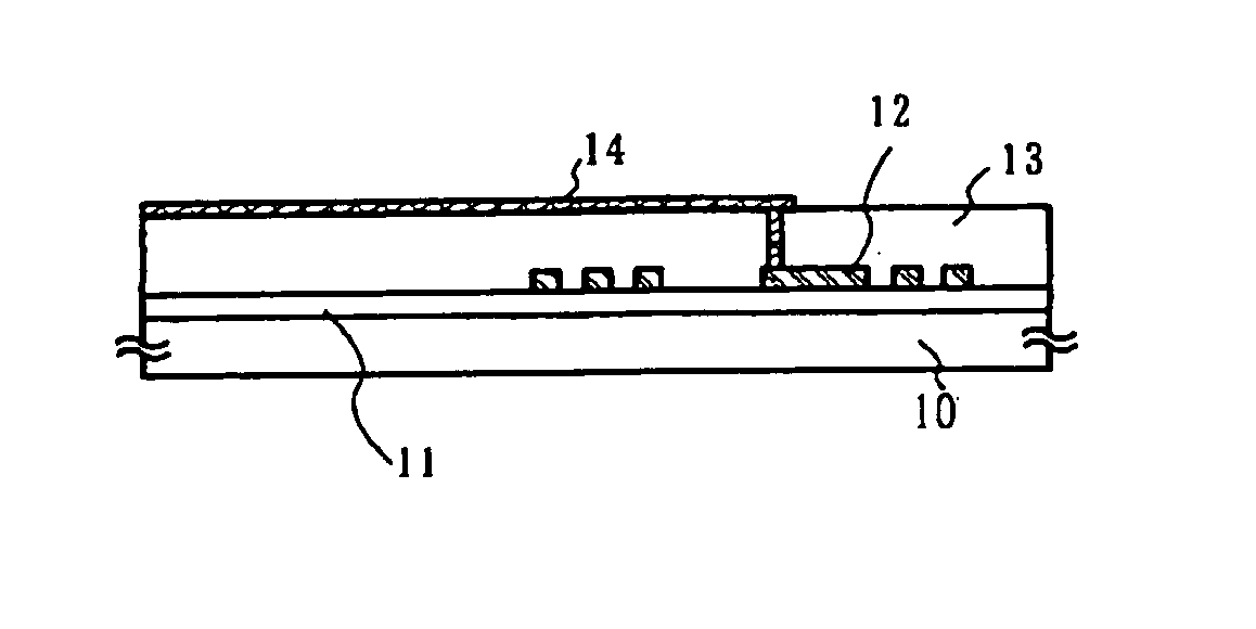
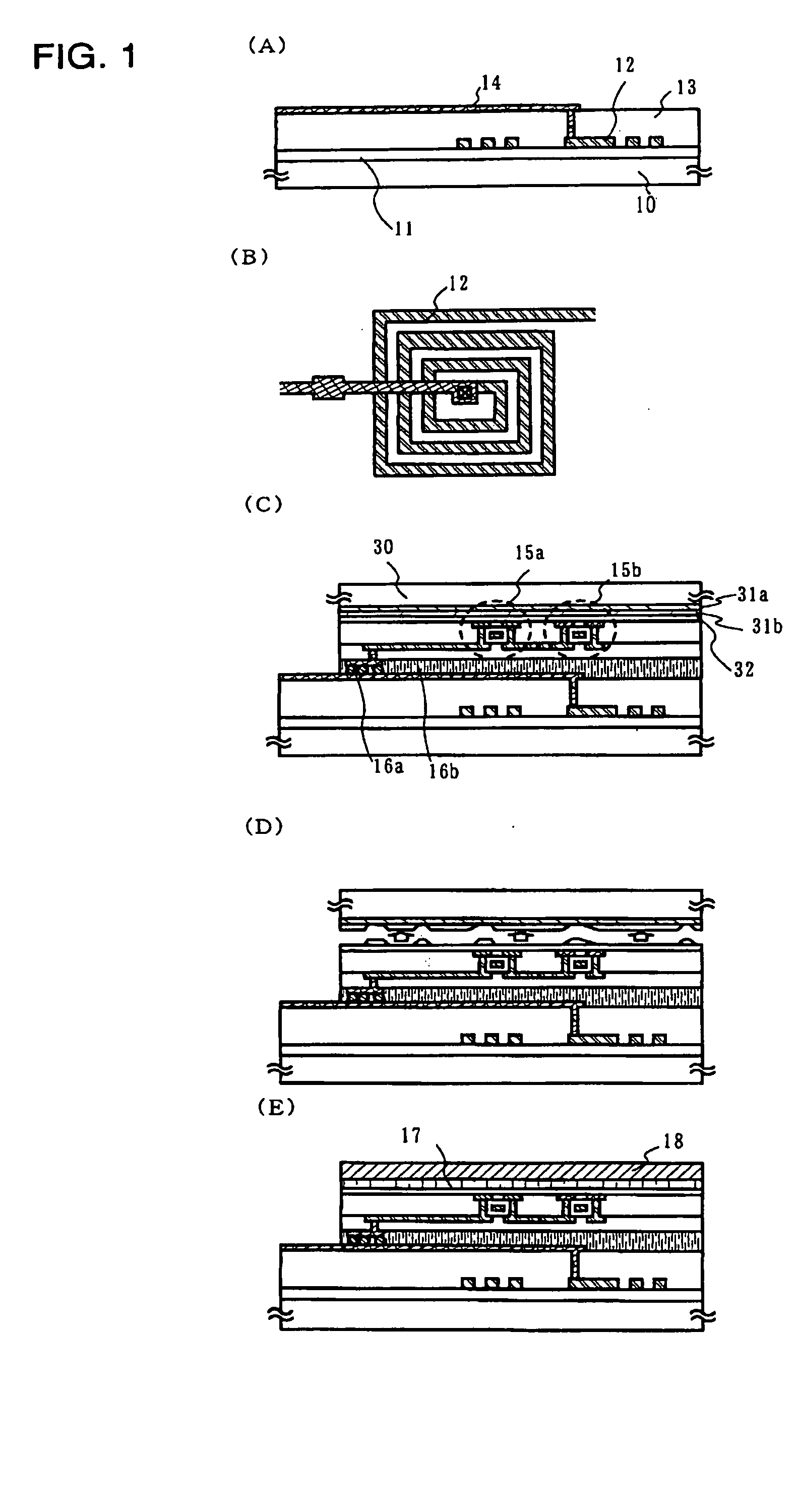
[0060] An example is shown here, in which a laminated capacitor or a laminated inductor is formed without using a semiconductor substrate, transferred to and mounted on a circuit board (printed board).

[0061] First, a heat-resisting glass substrate (e.g. a quartz substrate) or a ceramics substrate is prepared.

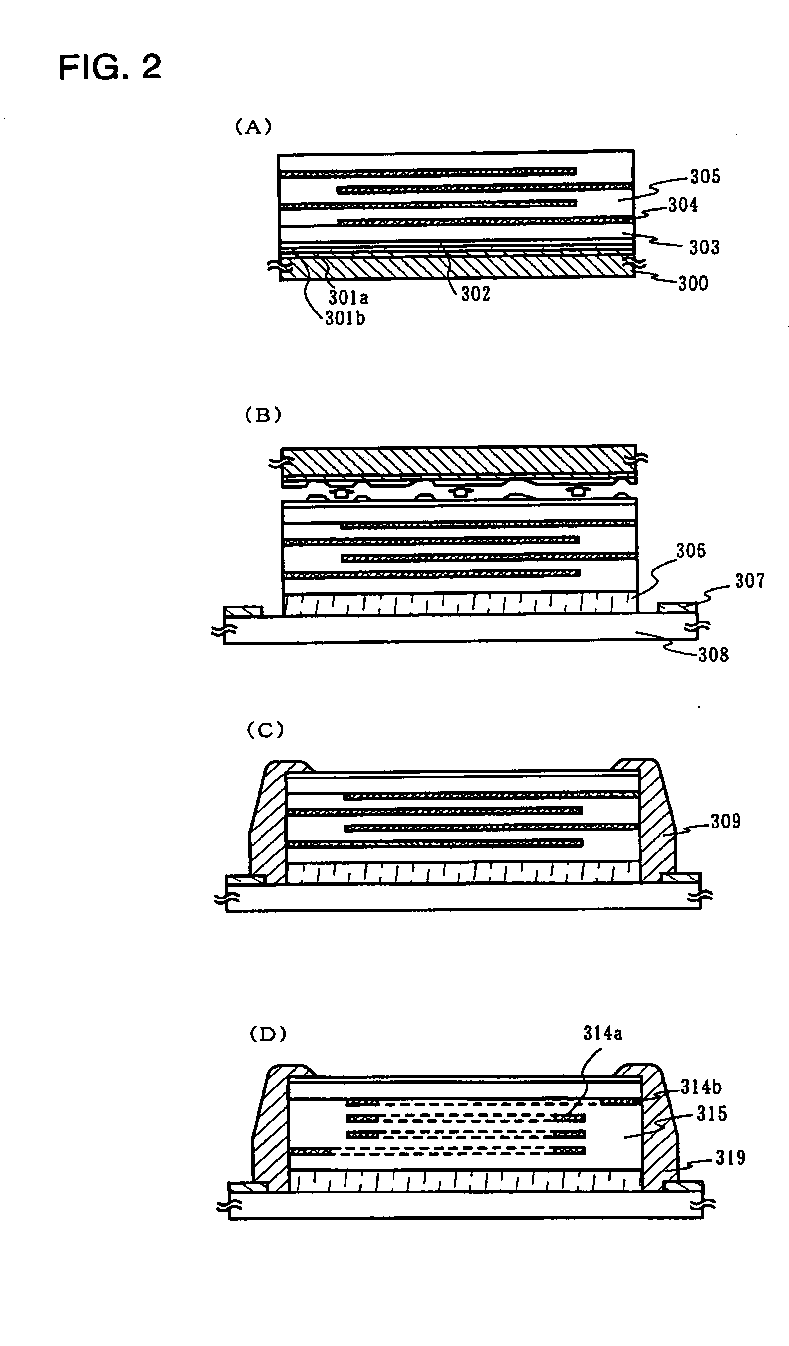
[0062] An example which a laminated capacitor is formed on a substrate (a first substrate 300) is described with reference to FIGS. 2(A) to 2 (C). A ceramic substrate is employed in this embodiment since baking at a high temperature is performed. A metal film 301a, here, a tungsten film (from 10 nm to 200 nm in the film thickness, preferably, from 50 nm to 75 nm) is formed by a sputtering method on this ceramic substrate, and further, an oxide film 302, here a silicon oxide film (from 150 nm to 200 nm in the film thickness) is laminated without being exposed to the air. The film thickness of the oxide film 302 is preferably equal to or more than twice t...

embodiment 1

[0199] Embodiment 1

[0200] A cellular phone having a GPS function is described as an example in this embodiment with reference to FIG. 10.

[0201] In FIG. 10(A), functional circuits such as an antenna, a receiver circuit, a transmitting circuit, and a GPS are formed, and further, a flash memory memorizing call-register, a camera controller, a controller connected to a display panel, a RAM and the like are provided. In addition, an amplifier for amplifying a signal from a microphone, an amplifier for amplifying a signal for outputting audio to a loudspeaker and the like are provided. Moreover, a CPU to be connected to them is provided.

[0202] According to the present invention, a circuit in the portion surrounded by a dotted line in FIG. 10(A) can be manufactured and mounted on a circuit board without using a semiconductor substrate. A capacitor, an inductor, a resistor element, a SAW element and the like that are each obtained according to any one of Embodiment Modes 1 to 7 are combin...

embodiment 2

[0209] Embodiment 2

[0210] In FIG. 13(A), reference numeral 1001 denotes a central processing unit (also, referred to as a CPU), 1002 denotes a control unit, 1003 denotes an operation part, 1004 denotes a memory unit (referred to as a memory), 1005 denotes an input unit, and 1006 denotes an output unit (such as a display portion).

[0211] The central processing unit 1001 includes the control unit 1002 and the arithmetic unit 1003. The operation part 1003 comprises an arithmetic logic unit (ALU) for performing arithmetic operations such as addition and subtraction, or logical operations such as AND, OR, and NOT, various registers for temporarily storing data or results of the operations, a counter for counting the number of 1 that are inputted, and the like. Circuits constituting the operation part 1003, such as an AND circuit, an OR circuit, a NOT circuit, a buffer circuit, a resistor circuit, can be formed from TFTs. For the sake of obtaining a high field effect mobility, a semicondu...


PUM


Abstract

It is an object to provide a semiconductor device integrating various elements without using a semiconductor substrate, and a method of manufacturing the same. According to the present invention, a layer to be separated including an inductor, a capacitor, a resistor element, a TFT element, an embedded wiring and the like, is formed over a substrate, separated from the substrate, and transferred onto a circuit board 100. An electrical conduction with a wiring pattern 114 provided in the circuit board 100 is made by a wire 112 or a solder 107, thereby forming a high frequency module or the like.

Description

BACKGROUND OF THE INVENTION [0001] 1. Field of the Invention [0002] The present invention relates to a TFT, a resistor element, an LC element attenuating a predetermined frequency band, a semiconductor device on which an integrated circuit combining these elements is mounted, and a method of manufacturing the same. [0003] Note that a semiconductor device in this specification means general devices which can function by using semiconductor characteristics, and all of electro-optic devices, semiconductor circuits and electronic devices are the semiconductor devices. [0004] 2. Description of the Related Art [0005] A high frequency integrated circuit (also referred to as MMIC) in which an active element such as a transistor and a passive element such as a capacitor, a resistor or an inductor are formed on one semiconductor substrate is known. An active element such as a MESFET, a HEMT, or a HBT, and a lumped parameter element such as a capacitor, an inductor, or a resistor, and a distri...

Claims


Application Information

Patent Timeline
IPC IPC(8): H01L21/336H01L21/60H01L21/68H01L23/538H01L27/06H01L27/12H03H3/08
CPCH01L21/6835H01L23/5385H01L23/5388H01L24/81H01L27/0688H01L27/12H01L29/66757H01L2221/68354H01L2221/68359H01L2221/68363H01L2221/68368H01L2224/16145H01L2224/32145H01L2224/48091H01L2224/81801H01L2924/01012H01L2924/01013H01L2924/01025H01L2924/01029H01L2924/0103H01L2924/01046H01L2924/01056H01L2924/0106H01L2924/01073H01L2924/01077H01L2924/01078H01L2924/01079H01L2924/01082H01L2924/14H01L2924/1423H01L2924/15311H01L2924/19041H01L2924/19042H01L2924/19043H01L2924/3011H03H3/08H01L2224/16225H01L2224/32225H01L2224/48227H01L2224/73265H01L2924/13063H01L24/48H01L2924/01005H01L2924/01006H01L2924/01023H01L2924/01024H01L2924/01033H01L2924/01041H01L2924/01042H01L2924/01045H01L2924/01047H01L2924/0105H01L2924/01055H01L2924/01074H01L2924/01087H01L2924/014H01L2224/92247H01L2924/19105H01L2224/73204H01L2924/10253H01L2924/13064H01L2924/00014H01L2924/00H01L2924/00012H01L2924/15787H01L2924/15788H01L2924/181H01L2924/12034H01L2924/12042H01L24/73H01L2224/45099H01L2224/45015H01L2924/207
Inventor YAMAZAKI, SHUNPEITAKAYAMA, TORUMARUYAMA, JUNYAOHNO, YUMIKOGOTO, YUUGOKUWABARA, HIDEAKI
Owner SEMICON ENERGY LAB CO LTD
Why Eureka
Try Eureka