Further method to pattern a substrate

a substrate and patterning technology, applied in the field of patterning substrates, can solve the problems of reducing lithographic performance, reducing criticality, and moving from traditional dnq/novolak based to chemically amplified resist processing,

Inactive Publication Date: 2005-03-10
MICRONIC LASER SYST AB
View PDF3 Cites 74 Cited by
  • Summary
  • Abstract
  • Description
  • Claims
  • Application Information

AI Technical Summary

Benefits of technology

Accordingly, it is an object of the present invention to provide a method of producing small features on a substrate with precise critical dimension.

Problems solved by technology

However, a difference in criticality is much less than might be expected and will in the near future disappear.
For laser pattern generators, the move from traditional DNQ / Novolak based towards DUV chemically amplified resist processing was initially troublesome.
The relative long total exposure time of pattern generators in contrast to wafer steppers, in combination with thick quartz substrates with relatively low heat capacity, may result in reduced lithographic performance due to excessive diffusion of photogenerated acid.
At the same time, the mask error enhancement factor is likely to increase due to more aggressive lithographic process trade-offs, such as tuning the lithographic process to optimize the manufacture of contact holes, transistors or other critical features in order to use feature sizes closer to the theoretical resolution limit.

Method used


Image

  • Further method to pattern a substrate
  • Further method to pattern a substrate
  • Further method to pattern a substrate

Examples


Embodiment Construction

The following detailed description is made with reference to the figures. Preferred embodiments are described to illustrate the present invention, not to limit its scope, which is defined by the claims. Those of ordinary skill in the art will recognize a variety of equivalent variations on the description that follows.

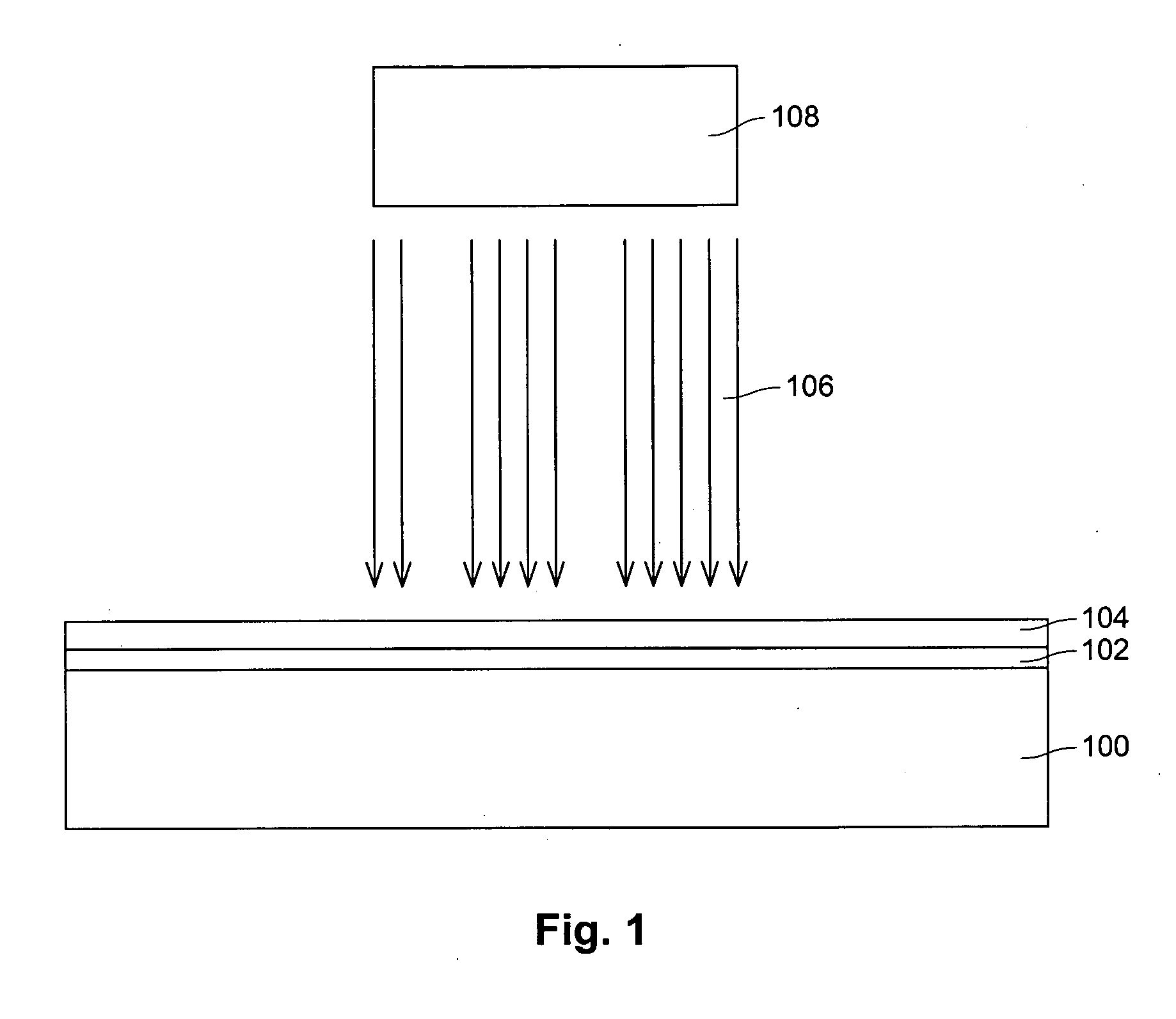
FIG. 1 depicts a coated substrate 100 including a masking or non-transmissive layer 102 and a resist layer 104. The substrate 100 may be a quartz substrate, an Erodent ceramic substrate or an ULE™ glass substrate when said substrate is to be a reticle or mask. However, when making integrated circuits by direct writing, said substrate may by any kind of semiconducting material. In such case the resist is applied directly onto said substrate.

The mask is formed over the transmissive substrate to block the passage of an energy beam in areas where resist on a wafer are intended not to be exposed. Unmasked portions of the substrate 100 allow an energy beam to pass throug...


PUM

PropertyMeasurementUnit
feature sizeaaaaaaaaaa
thickaaaaaaaaaa
exposure thresholdaaaaaaaaaa

Abstract

The present invention relates to methods for patterning substrates, such as reticles, masks or wafers, which reduce critical dimension variations, improving CD uniformity. In particular, it relates to tuning doses applied in passes of a multipass writing strategy to measurable characteristics of resists or radiation sensitive layers applied to the substrates. Particular writing strategies are described. Aspects of the present invention are described in the claims, specification and drawings.

Description

BACKGROUND OF THE INVENTION The present invention relates to methods for patterning substrates, such as reticles, masks or wafers, which reduce critical dimension variations, improving CD uniformity. In particular, it relates to tuning doses applied in passes of a multipass writing strategy to measurable characteristics of resists or radiation sensitive layers applied to the substrates. Particular writing strategies are described. Semiconductor devices include multiple layers of structure. The structures are formed in numerous steps, including steps of applying resist, then exposing, developing and selectively removing the resist to from a pattern of exposed areas. The exposed areas may be etched to remove material or sputtered to add material. A critical part of forming the pattern in the resist is exposing it. Resist is exposed to an energy beam that changes its chemical properties. One way of exposing the resist is with a stepper. The stepper uses a reticle, which typically in...

Claims


Application Information

Patent Timeline
Patent Type & Authority Applications(United States)
IPC IPC(8): G03C5/00G03F7/20
CPCG03F7/70558G03F7/70291G03C5/00G03F7/20
Inventor ASKEBJER, PERFOSSHAUG, HANSEKLUND, ROBERTWALFORD, JONATHAN
Owner MICRONIC LASER SYST AB
Why Eureka
Try Eureka