

Semiconductor memory device
a memory device and semiconductor technology, applied in the direction of solid-state devices, transistors, instruments, etc., can solve the problems of signal amount reduction, achieve high-speed and stable operation, reduce the level of word-line voltage, and accelerate the reading of “l” data
- Summary
- Abstract
- Description
- Claims
- Application Information
AI Technical Summary
Benefits of technology
Problems solved by technology
Method used
Image

Examples
Embodiment Construction
[0071] Hereinafter, an embodiment of the present invention will be described in detail with reference to the accompanying drawings. Note that components having the same functions are denoted by the same reference symbols throughout the drawings for describing the embodiment and the repetitive description thereof will be omitted.
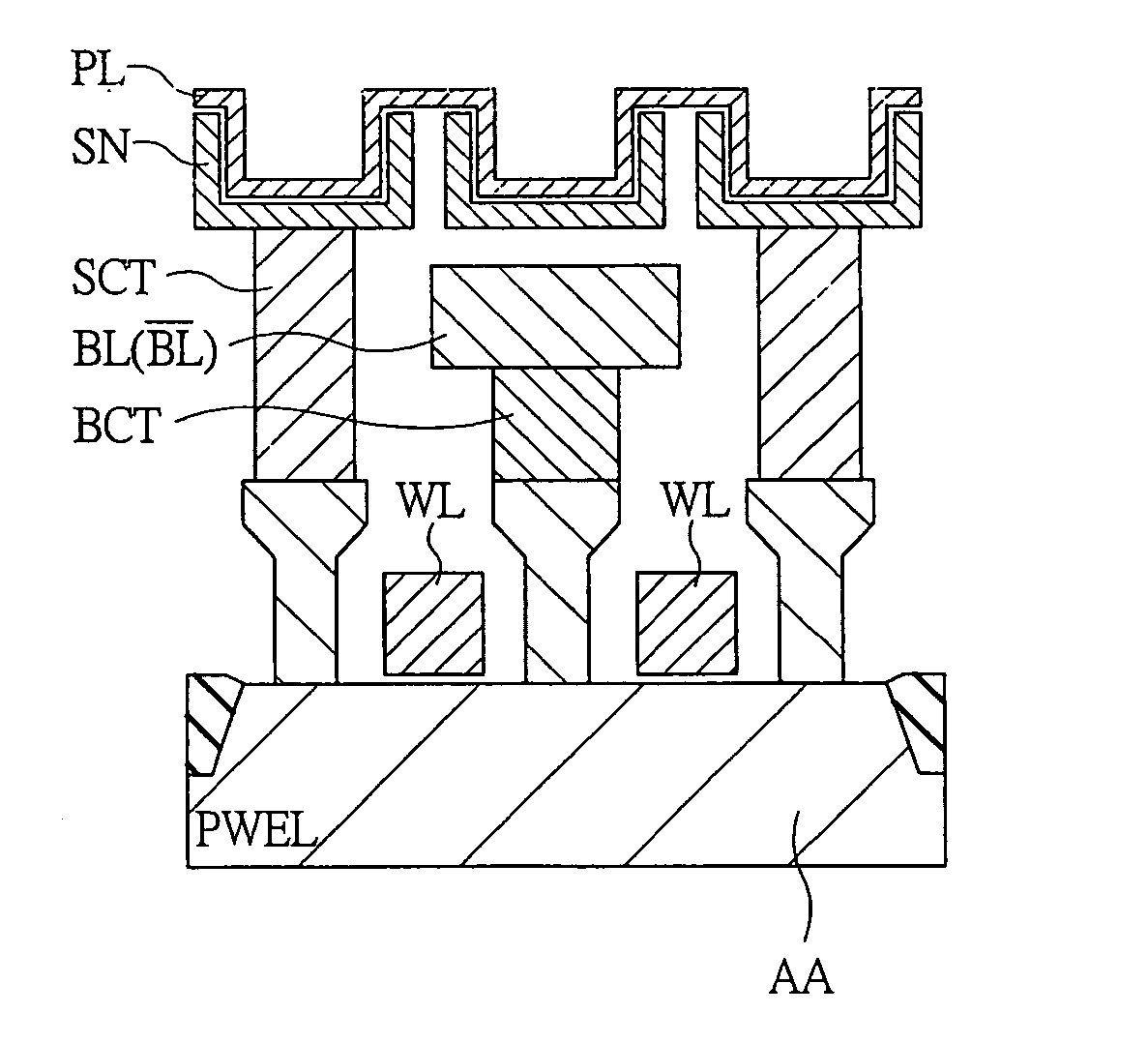
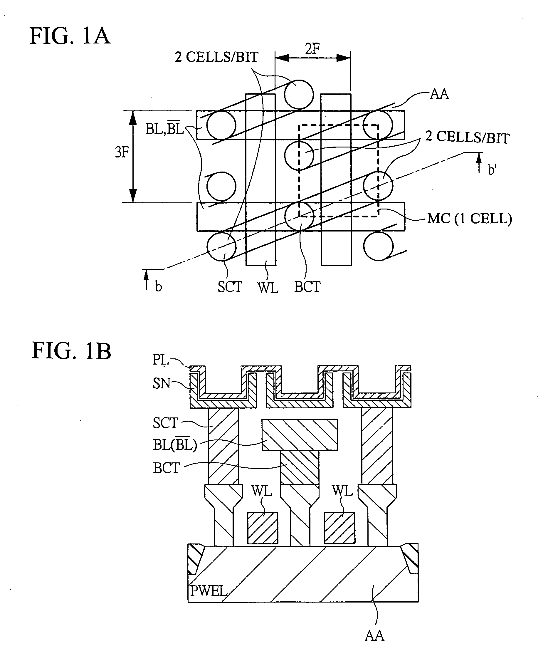
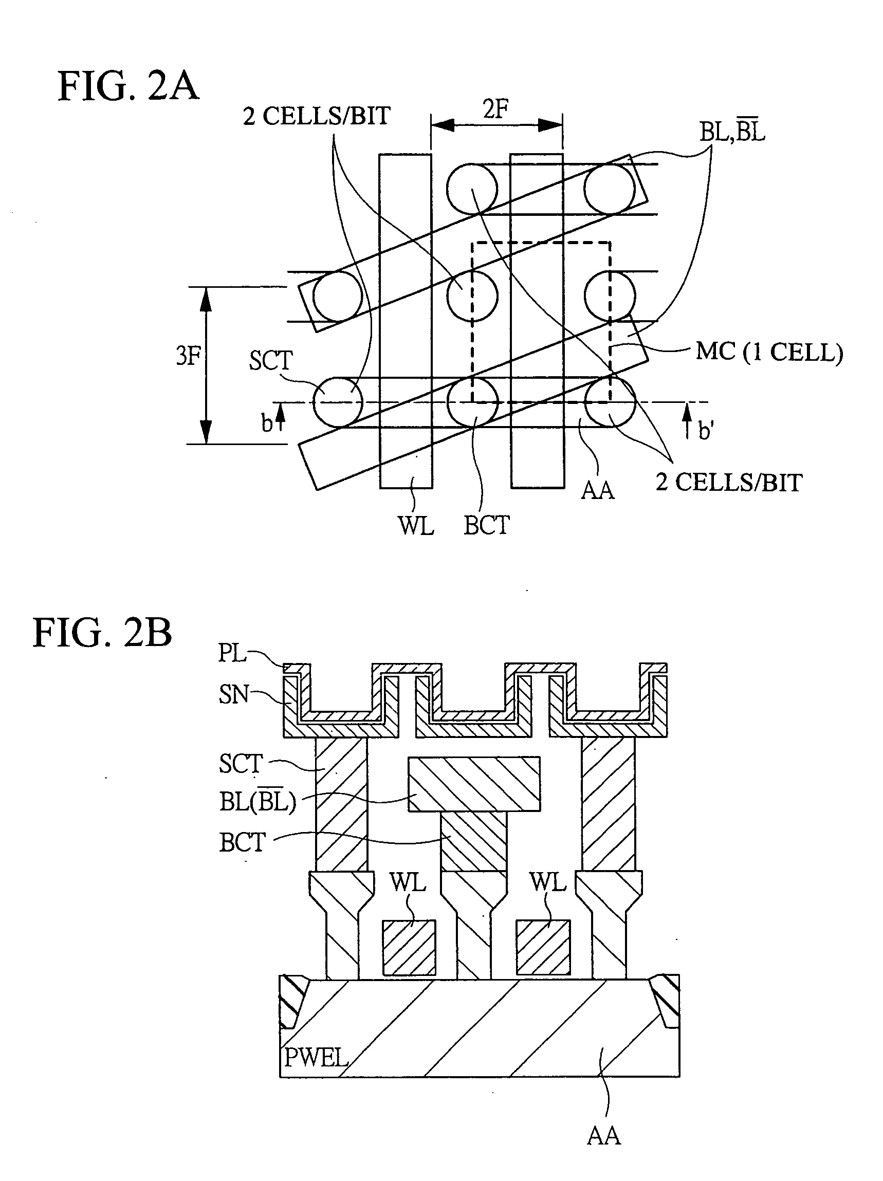
[0072] The semiconductor memory device according to an embodiment of the present invention is applied to, for example, a DRAM employing a one-intersection·two cells / bit method, and, though not particularly limited, is formed on one semiconductor substrate like single crystal silicon by a known semiconductor manufacturing technique. Particularly, the DRAM according to the embodiment is characterized by: 1. a twin cell structure employing a one-intersection 6 F2 cell; 2. a direct sense+twin cell method; and 3. a substrate potential VSS+twin cell method, etc. and they will be sequentially described below.
[0073] 1. Twin Cell Structure Employing One-Intersection...
PUM
 Abstract
Description
Claims
Application Information