Method of manufacturing Group III nitride crystal substrate, etchant used in the method, Group III nitride crystal substrate, and semiconductor device including the same

Inactive Publication Date: 2005-03-17
PANASONIC CORP +1
View PDF2 Cites 42 Cited by
  • Summary
  • Abstract
  • Description
  • Claims
  • Application Information

AI Technical Summary

Benefits of technology

The manufacturing method of the present invention can provide a Group III nitride crystal substrate having reduced strain and defects that are caused through the processin

Problems solved by technology

The Group III nitride crystal substrate, however, is h

Method used


Image

  • Method of manufacturing Group III nitride crystal substrate, etchant used in the method, Group III nitride crystal substrate, and semiconductor device including the same
  • Method of manufacturing Group III nitride crystal substrate, etchant used in the method, Group III nitride crystal substrate, and semiconductor device including the same
  • Method of manufacturing Group III nitride crystal substrate, etchant used in the method, Group III nitride crystal substrate, and semiconductor device including the same

Examples


embodiment 1

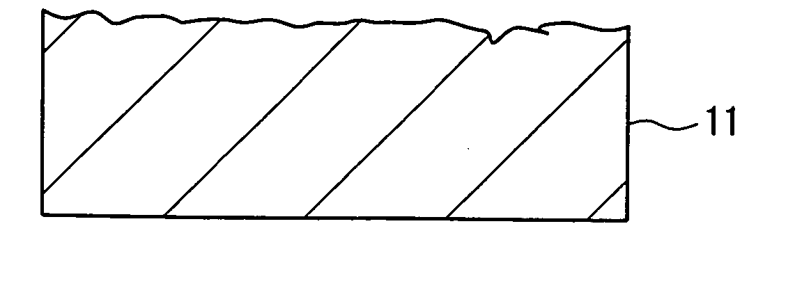
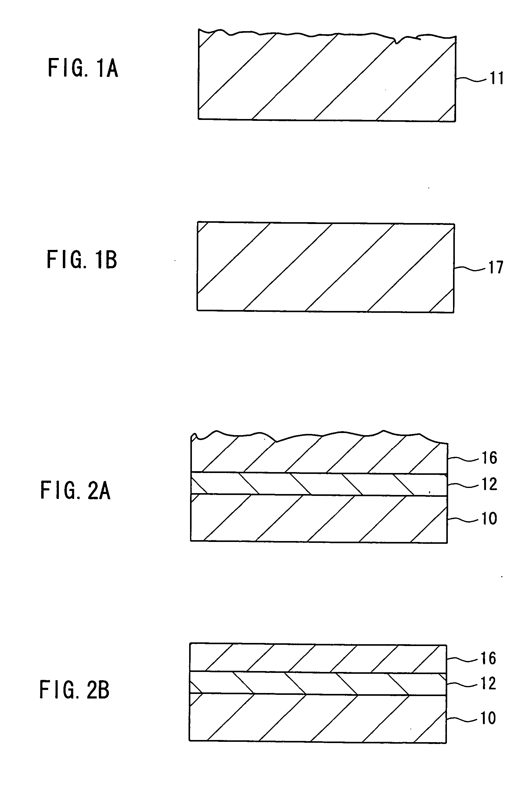
Embodiment 1 is directed to a manufacturing method including: a process of mechanically processing the surface of a Group III nitride crystal substrate including a semiconductor seed layer, a first semiconductor layer, and a second semiconductor layer; and an processing process that is carried out through meltback etching by bringing the surface processed mechanically into contact with a melt containing at least one of alkali metal and alkaline-earth metal.

First, a semiconductor seed layer (expressed by a composition formula of AlsGatIn1-s-tN (where 0≦s≦1, 0≦t≦1, and s+t≦1)) to serve as seed crystals is grown on a base substrate by, for instance, the vapor phase growth method such as the MOCVD.

Next, a first semiconductor layer that is expressed by a composition formula of AlmGanIn1-m-nN (where 0≦m≦1, 0≦n≦1, and m+n≦1) is grown through liquid phase growth on the semiconductor seed layer. Further, a second semiconductor layer that is expressed by a composition formula of AlxGayIn...

embodiment 2

Embodiment 2 is directed to an example of carrying out a surface treatment using the mechanochemical polishing of the present invention instead of the meltback etching of Embodiment 1.

A melt including at least one of alkali metal and alkaline-earth metal is prepared in the same manner as in the case of the meltback etching of Embodiment 1. Preferably, the melt includes a Group III element. It also is preferable that in the composition of the melt, for instance, one of the following formulae is satisfied:

0≦A / (A+M)≦0.10  (1); and

0.9≦A / (A+M)≦0.999  (2),

where “A” denotes the number of moles of the Group III element and “M” denotes the number of total moles of the alkali metal and alkaline-earth metal.

Such compositions allow the mechanochemical polishing of the present invention to be carried out at still lower temperatures. Polishing grains to be used herein are, for instance, alumina, diamond, or SiC that is relatively hard and has low reactivity with alkali metal and the like...

embodiment 3

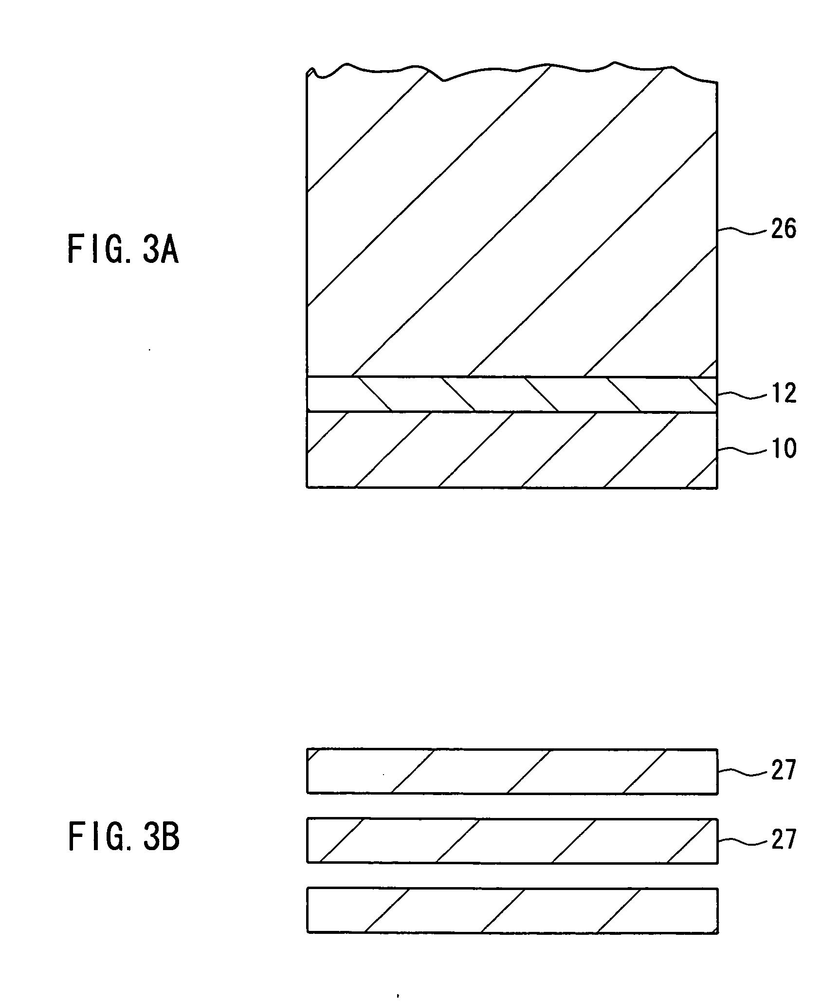
Embodiment 3 is directed to an example of the method of manufacturing a Group III nitride crystal substrate, which further includes, in addition to the processes of Embodiment 1, a process of removing at least the semiconductor seed layer and the first semiconductor layer from the base substrate side.

As in Embodiment 1, when a first semiconductor layer that is a high defect layer is formed between a semiconductor seed layer to serve as seed crystals and a second semiconductor layer that is a low defect layer, the high defect layer often has a considerably different carrier density and contains a large amount of impurities. Hence, it may be preferable that the high defect layer is removed when a device is to be produced using the substrate. The reason for this is as follows. That is, particularly in the case of, for example, a semiconductor laser, electrodes may be formed on the rear face of the substrate and in that case, the presence of the part that is considerably different in...


PUM


Abstract

The present invention provides a Group III nitride crystal substrate whose surface has concavities and convexities reduced in size. The surfaces with concavities and convexities, such as hillocks, pits and facets, of Group III nitride crystals are brought into contact with a melt and thereby the surfaces are subjected to meltback etching or mechanochemical polishing. The melt includes at least one of alkali metal and alkaline-earth metal. Thus a Group III nitride crystal substrate that has reduced strain and a reduced number of defects, which are caused through the processing, and is excellent in surface flatness is manufactured. Furthermore, by the use of the Group III nitride crystal substrate of the present invention, for instance, semiconductor devices of high performance can be obtained.

Description

BACKGROUND OF THE INVENTION 1. Field of the Invention The present invention relates generally to a method of manufacturing a Group III nitride crystal substrate, an etchant to be used in the method, a Group III nitride crystal substrate, and a semiconductor device with the same. 2. Related Background Art A Group III nitride compound semiconductor such as, for instance, gallium nitride (GaN) (hereinafter also referred to as a “Group III nitride semiconductor” or a “GaN-based semiconductor”) has been gaining attention as a material for semiconductor devices that emit green, blue or ultraviolet light. A laser diode (LD) that emits blue light is used for high-density optical disk devices or displays while a light emitting diode (LED) that emits blue light is used for displays, lighting, etc. It is expected to use an ultraviolet LD in the field of, for example, biotechnology and an ultraviolet LED as, for example, an ultraviolet source for a fluorescent lamp. Generally, Group III ni...

Claims


Application Information

Patent Timeline
IPC IPC(8): C30B19/02C30B29/40H01L21/20H01L21/205H01L21/208H01L21/28H01L21/304H01L21/306
CPCC30B19/02C30B29/40H01L21/30612H01L21/30625H01L21/02664H01L21/0242H01L21/02458H01L21/0254H01L21/0262H01L21/02389
Inventor MINEMOTO, HISASHIKITAOKA, YASUOKIDOGUCHI, ISAOMORI, YUSUKESASAKI, TAKATOMOKAWAMURA, FUMIO
Owner PANASONIC CORP
Why Eureka
Try Eureka