
Method for reducing the effective thickness of gate oxides by nitrogen implantation and anneal

a technology of nitrogen implantation and gate oxide, which is applied in the direction of semiconductor devices, basic electric elements, electrical equipment, etc., can solve the problems of increasing affecting the performance of the device, and affecting the device performance, so as to reduce the effective thickness prevent the diffusion of dopant, and increase the dielectric constant of the gate oxide layer

Inactive Publication Date: 2005-03-24
MICRON TECH INC
View PDF18 Cites 6 Cited by
  • Summary
  • Abstract
  • Description
  • Claims
  • Application Information

AI Technical Summary

Benefits of technology

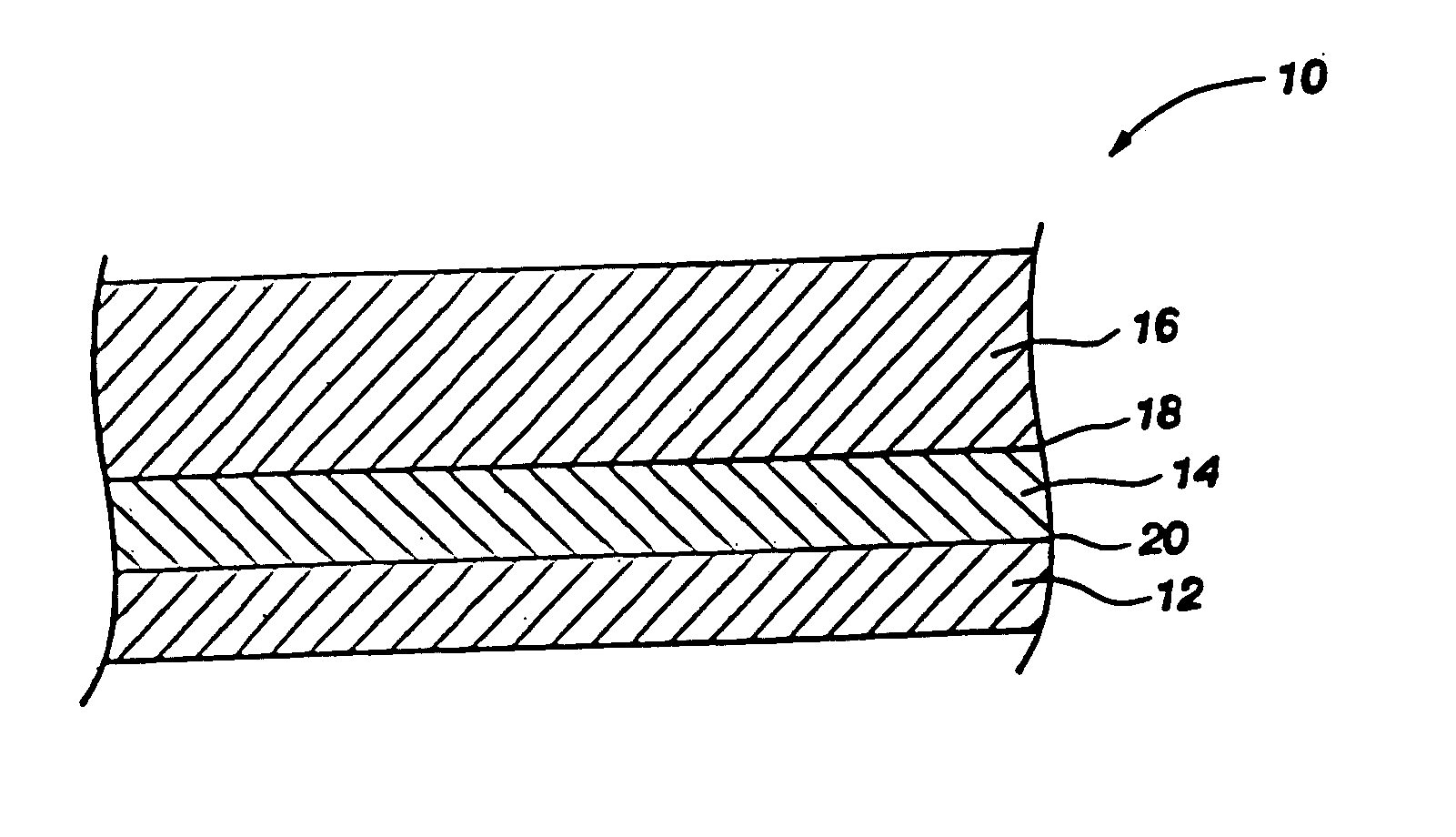
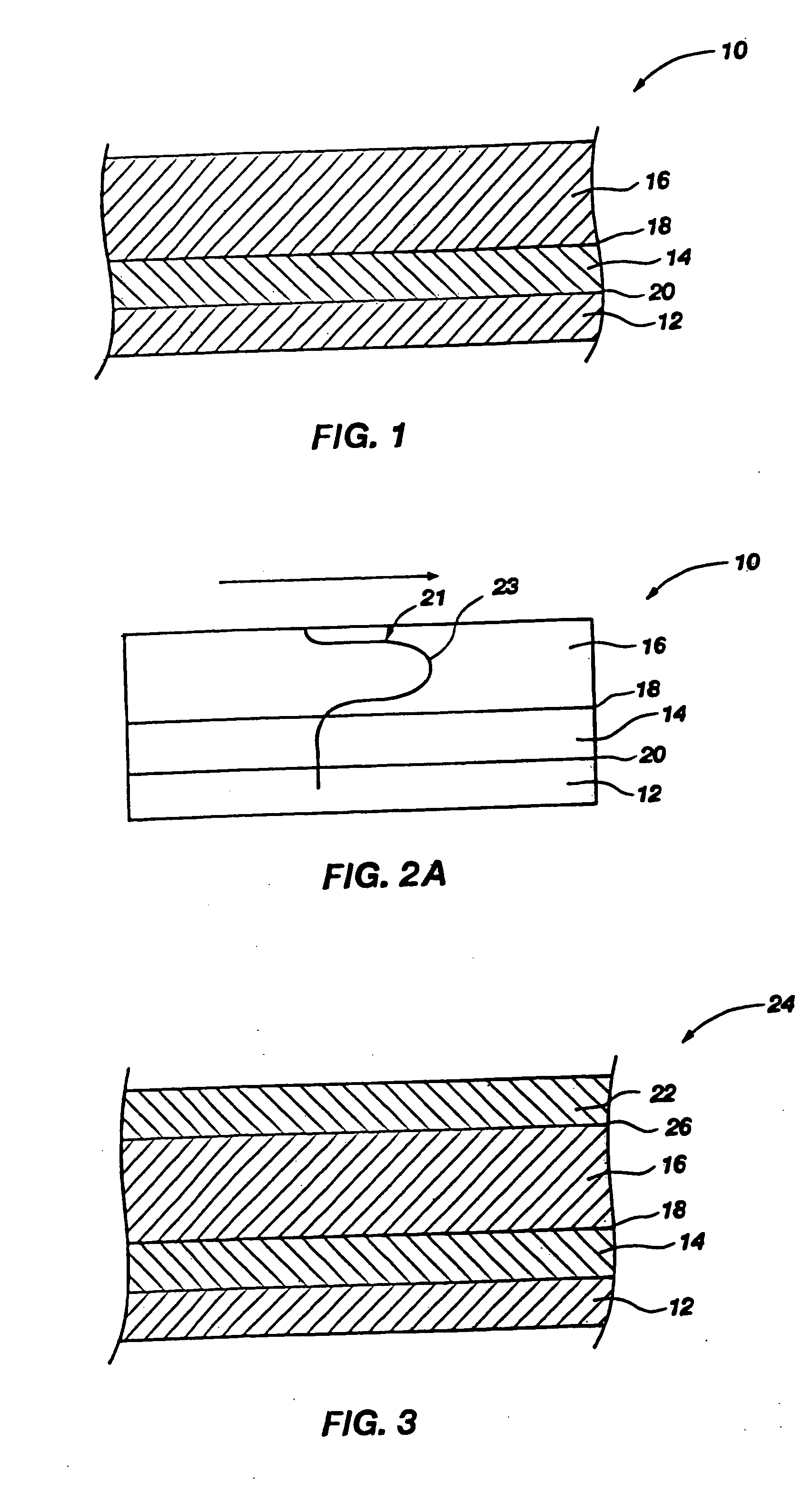
[0015] In a semiconductor device having a gate oxide hardened utilizing the method of the present invention, the nitrogen at the polysilicon / gate oxide interface acts as a diffusion barrier to prevent diffusion of dopants from the polysilicon layer into and through the gate oxide layer. Additionally, nitrogen concentrated at the gate oxide / substrate interface also aids in preventing dopant diffusion; however, this concentration is not so great as to substantially impair device performance. Further, the nitrogen within the gate oxide layer reacts with the pure oxide to form oxynitride, which has an increased dielectric constant. Accordingly, the effective thickness of the gate oxide layer is reduced.
[0017] In a semiconductor device having a metal gate strap and a gate oxide hardened utilizing the method of the present invention, the nitrogen concentrated at the silicide / polysilicon interface acts to substantially prevent cross-diffusion of dopants across the interface and the concentration of nitrogen at the polysilicon / gate oxide interface acts as a diffusion barrier to prevent diffusion of dopants from the polysilicon layer into and through the gate oxide layer. Nitrogen concentrated at the gate oxide / substrate interface also aids in preventing dopant diffusion; however, this concentration is not so great as to substantially impair device performance. Further, the nitrogen within the gate oxide layer reacts with the pure oxide to form oxynitride and, accordingly, increases the dielectric constant of the gate oxide layer and reduces the effective thickness thereof.

Problems solved by technology

Additionally, nitrogen concentrated at the gate oxide / substrate interface also aids in preventing dopant diffusion; however, this concentration is not so great as to substantially impair device performance.
Nitrogen concentrated at the gate oxide / substrate interface also aids in preventing dopant diffusion; however, this concentration is not so great as to substantially impair device performance.
Further, the nitrogen within the gate oxide layer reacts with the pure oxide to form oxynitride and, accordingly, increases the dielectric constant of the gate oxide layer and reduces the effective thickness thereof.

Method used


Image

  • Method for reducing the effective thickness of gate oxides by nitrogen implantation and anneal
  • Method for reducing the effective thickness of gate oxides by nitrogen implantation and anneal
  • Method for reducing the effective thickness of gate oxides by nitrogen implantation and anneal

Examples


example

[0040] A gate oxide layer having a thickness of about 30 angstroms was thermally grown over a silicon substrate using methods known to those of ordinary skill in the art. A layer of polysilicon having a thickness of about 600 angstroms was subsequently deposited over the gate oxide layer followed by deposition of a layer of tungsten silicide having a thickness of about 600 angstroms atop the polysilicon layer. The dielectric constant of the gate oxide was determined and recorded.

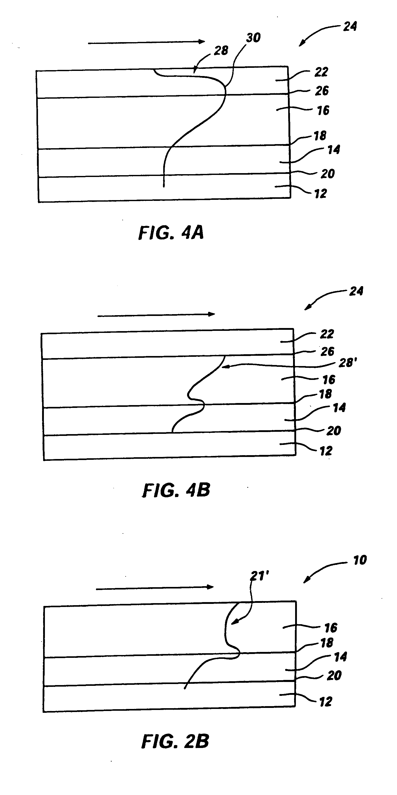
[0041] Nitrogen was subsequently implanted into the gate stack, at room temperature, at a dosage of about 4×10¹⁵ atoms / cm2 and at an energy of about 30 keV. The resultant nitrogen-implanted gate stack had a nitrogen concentration profile approximating that illustrated in FIG. 4A with the bulk of the nitrogen concentration occurring within the metal silicide layer and in the polysilicon layer at the silicide / polysilicon interface while about 10% of the total amount of nitrogen implanted (i.e., about 4×10¹⁴ a...


PUM


Abstract

A method for reducing the effective thickness of a gate oxide using nitrogen implantation and anneal subsequent to dopant implantation and activation is provided. More particularly, the present invention provides a method for fabricating semiconductor devices, for example, transistors, which include a hardened gate oxide and which may be characterized by a relatively large nitrogen concentration at the polysilicon / gate oxide interface and a relatively small nitrogen concentration within the gate oxide and at the gate oxide / substrate interface. Additionally, the present invention provides a method for fabricating a semiconductor device having a metal gate strap (e.g., a metal silicide layer) disposed over the polysilicon layer thereof, which device includes a hardened gate oxide and which may be characterized by a relatively large nitrogen concentration at the silicide / polysilicon interface to substantially prevent cross-diffusion.

Description

CROSS-REFERENCE TO RELATED APPLICATION [0001] This application is a divisional of application Ser. No. 10 / 651,314, filed Aug. 28, 2003, pending.BACKGROUND OF THE INVENTION [0002] 1. Field of the Invention [0003] The present invention relates generally to semiconductor devices and methods for their fabrication. More particularly, the present invention relates to hardening of gate oxides in semiconductor devices by nitrogen implantation and anneal subsequent to dopant implantation and activation to increase the dielectric constant thereof and, accordingly, decrease the effective thickness of the gate oxide. [0004] 2. State of the Art [0005] Higher performance, enhanced reliability and greater packaging density are constant goals of the semiconductor industry. However, as components of integrated circuits become increasingly smaller to meet these goals, it has become more and more difficult to produce semiconductor devices capable of reliable, long-term operation, particularly in view ...

Claims


Application Information

Patent Timeline
Patent Type & Authority Applications(United States)
IPC IPC(8): H01L21/28H01L29/51
CPCH01L21/28052H01L21/28061H01L29/518H01L21/28194H01L21/28176
Inventor WANG, ZHONGZE
Owner MICRON TECH INC
Learn More