Gallium-nitride deposition substrate, method of manufacturing gallium-nitride deposition substrate,and method of manufacturing

Inactive Publication Date: 2005-03-24
SUMITOMO ELECTRIC IND LTD
View PDF3 Cites 31 Cited by
  • Summary
  • Abstract
  • Description
  • Claims
  • Application Information

AI Technical Summary

Benefits of technology

[0039] GaN deposition in which low-dislocation single crystal growth is kept up without increasing defects over the ELO mask F, and in which defects are concentrate

Problems solved by technology

SiO2 has demonstrated proven results as an ELO mask and thus has worked well for ELO deposition, but it has not worked well as the seeds for a defect-seeding mask.
Initially it was the case that a GaN layer

Method used


Image

  • Gallium-nitride deposition substrate, method of manufacturing gallium-nitride deposition substrate,and method of manufacturing
  • Gallium-nitride deposition substrate, method of manufacturing gallium-nitride deposition substrate,and method of manufacturing
  • Gallium-nitride deposition substrate, method of manufacturing gallium-nitride deposition substrate,and method of manufacturing

Examples


Example

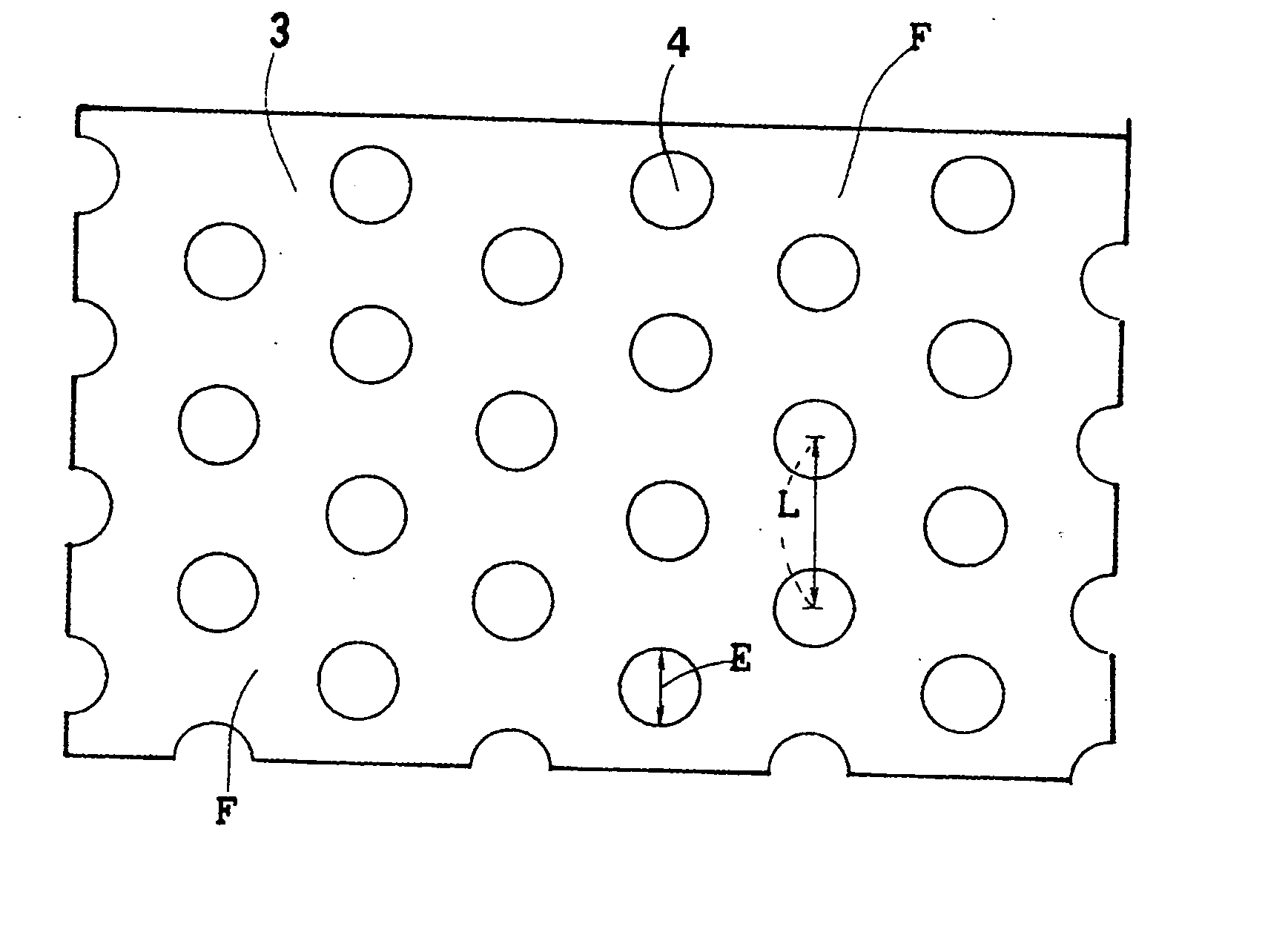
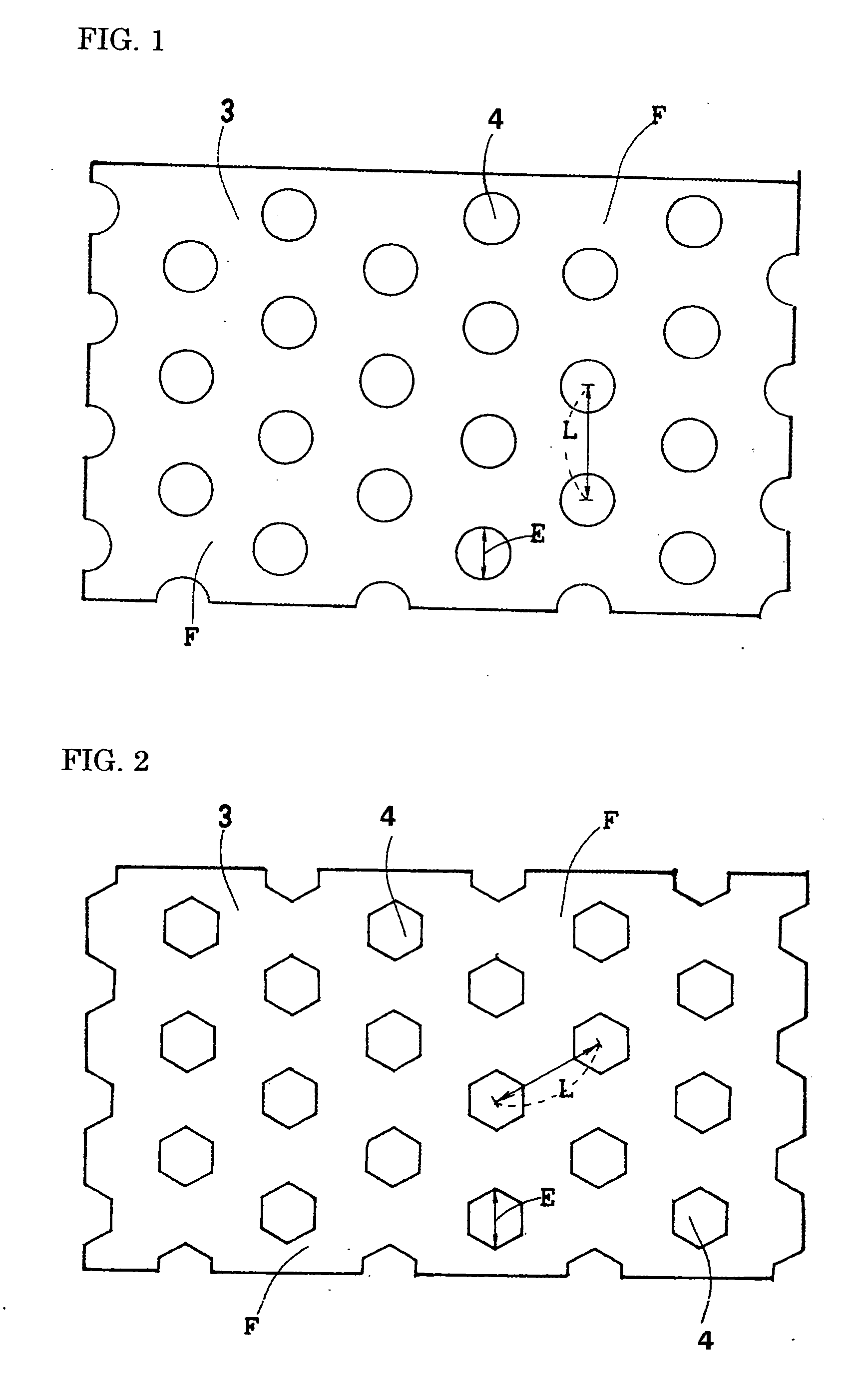
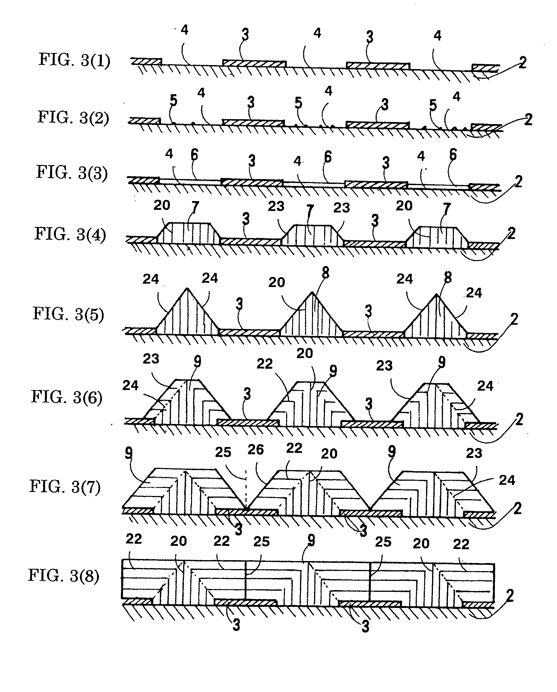
[0050] The present invention furnishes an ELO mask F for reducing initial-stage defects, and defect-seeding masks X that bring about defect concentration during growth, complementarily atop an under-substrate, and grows thereon thick-crystal GaN by means of vapor-phase deposition. Once a sufficiently thick GaN single crystal has been grown the under-substrate and masks are removed by polishing.

[0051] 1. Under-substrate—A single-crystal substrate that enables GaN growth is utilized: sapphire single crystal, GaAs single crystal, spinel single crystal, Si single crystal, InP single crystal, SiC single crystal, GaN single crystal, or an under-substrate in which a thin GaN buffer layer is formed superficially on one of these single crystals.

[0052] 2. ELO mask—May be SiN, SiON or SiO2. These dielectric layers are formed by sputtering or CVD. Film thickness is some 30 nm to 200 nm.

[0053] 3. Defect-seeding mask—May be Pt, Ti or Ni. These metal layers are formed by vapor deposition, sputt...


PUM


Abstract

GaN crystal having few dislocations is grown by using together ELO-mask and defect-seeding-mask means. ELO masks make it so that GaN crystal does not grow directly, but grows laterally; defect-seeding masks make it so that closed defect-gathering regions in which defects are concentrated are grown.
Any of the materials SiN, SiON or SiO2 is utilized for the ELO mask, while any of the materials Pt, Ni or Ti is utilized for the defect-seeding masks. With a sapphire, GaAs, spinel, Si, InP, SiC, etc. single-crystal substrate, or one in which a GaN buffer layer is coated onto a single-crystal substrate of these, as an under-substrate, the ELO mask and defect-seeding masks are provided complementarily and GaN is vapor-phase deposited.

Description

TECHNICAL FIELD [0001] This invention relates to gallium-nitride (GaN) single-crystal substrates employed as substrates for blue light-emitting diodes (LEDs) and blue laser diodes (LDs), and relates to methods of manufacturing the substrates. Nitride-system blue light-emitting devices are sometimes called InGaN-system light-emitting devices because their active layer is an InGaN film, and at times they are also referred to simply as GaN systems. Because manufacturing GaN single-crystal substrates is difficult, at present manufacture is by hetero-epitaxially growing GaN thin films, InGaAs thin films, etc. onto a hexagonal-system sapphire substrate. Sapphire-substrate InGaN LEDs have demonstrated positive results in use, and have proven satisfactory in terms of brightness, reliability, and lifespan. Substrates for the InGaN-system LEDs widely being used at present are for the most part sapphire substrates. In other words, they are said to be “on-sapphire” InGaN LEDs. [0002] Neverthele...

Claims


Application Information

Patent Timeline
IPC IPC(8): C30B25/02C30B25/18C30B29/40C30B29/38H01L21/20H01L21/205
CPCC30B25/02C30B25/18C30B29/406H01L21/02647H01L21/02458H01L21/0254H01L21/02639H01L21/0237C30B29/38
Inventor AKITA, KATSUSHIOKAHISA, TAKUJI
Owner SUMITOMO ELECTRIC IND LTD
Why Eureka
Try Eureka