Method for manufacturing a CMOS image sensor

a manufacturing method and image sensor technology, applied in the direction of diodes, radiation controlled devices, semiconductor devices, etc., can solve the problems of leakage current, high power consumption, complicated drive mode,

Active Publication Date: 2005-03-24
DONGBU HITEK CO LTD
View PDF25 Cites 145 Cited by
  • Summary
  • Abstract
  • Description
  • Claims
  • Application Information

AI Technical Summary

Benefits of technology

[0030] According to the characteristic construction of the present invention, by forming an ion anti-implantation layer (an “ion implantation barrier layer”) for restraining or preventing ion penetration into or through a gate electrode, when dopant ions for forming a subsequent low-concentration dopant region for a photodiode are implanted, even though a photosensitive layer pattern formed as an ion implantation mask is not exactly aligned with a gate electrode pattern or an ion implantation barrier layer pattern, the low-concentration dopant region formed by ion implantation is prevented from overlapping with a lower region (e.g., a channel) of the gate electrode.

Problems solved by technology

The CCD has various disadvantages, such as complicated drive mode, much power consumption, impracticability or impossibility of fabricating a signal processing circuit in the same chip as the CCD due to many mask processes, and so on.
As a result, short channel effects and possibly other detriments) are incurred, which can generate a leakage current.

Method used


Image

  • Method for manufacturing a CMOS image sensor
  • Method for manufacturing a CMOS image sensor
  • Method for manufacturing a CMOS image sensor

Examples


Embodiment Construction

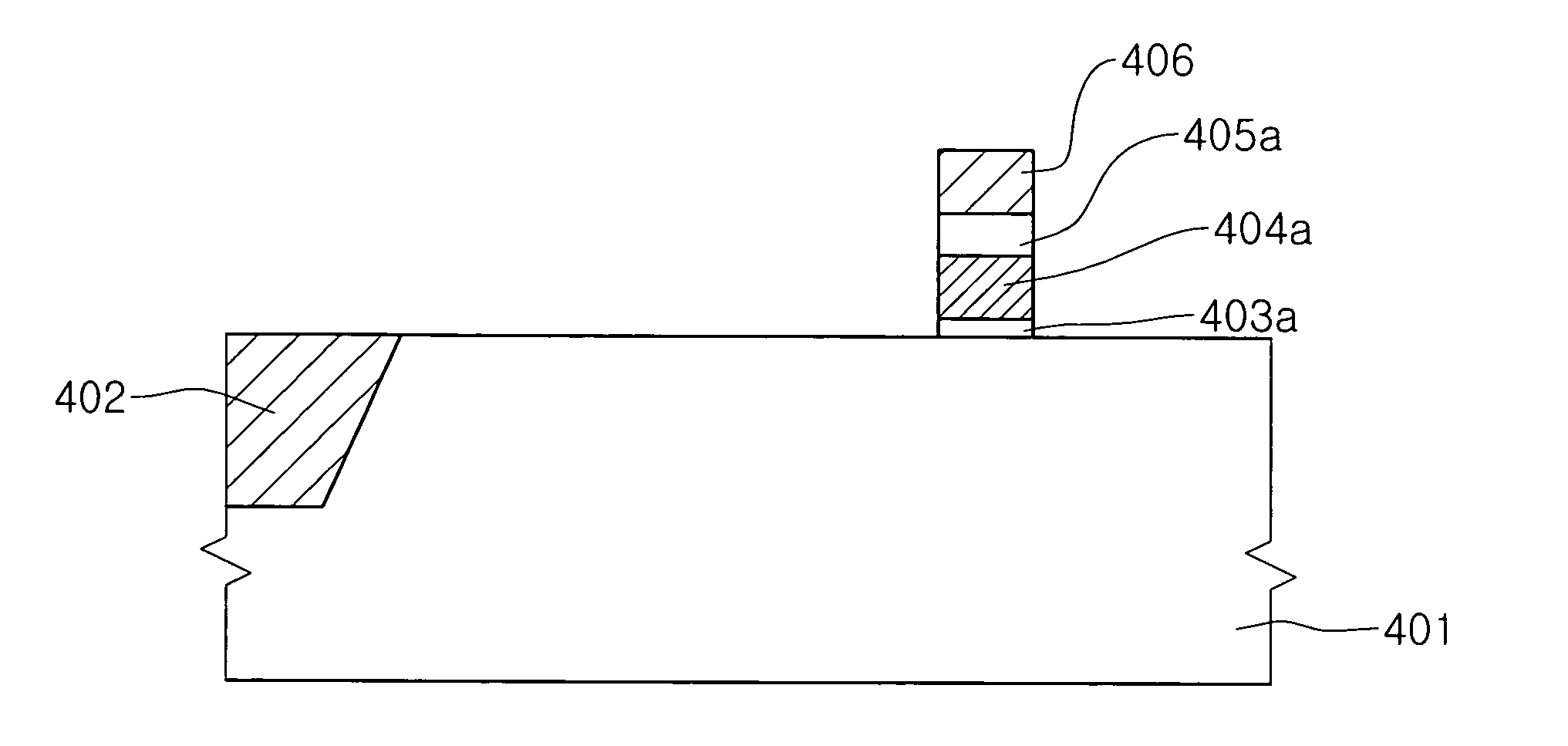
[0036] Hereinafter, a method for manufacturing a CMOS image sensor according to the present invention will be described in detail with reference to the accompanying drawings. FIGS. 4a to 4d are process sectional views for explaining a method for manufacturing a CMOS image sensor according to the present invention. Here, FIGS. 4a to 4d each correspond to a sectional view taken along line A-A′ of FIG. 2.

[0037] First, as shown in FIG. 4a, in order to provide electrical insulation between active regions of a semiconductor substrate 401, for example a p-type single crystalline silicon substrate, an element isolating layer 402 is formed on a field region of the semiconductor substrate, for example by a shallow trench isolation (STI) process. Here, the element isolation layer 402 may be formed by another conventional isolation process other than the STI process, for example a local oxidation of silicon (LOCOS) process. Meanwhile, even though not shown in the drawings, a p-type epitaxial l...


PUM


Abstract

A method for manufacturing structures of a CMOS image sensor. The method comprises the steps of depositing a gate insulating layer and a conductive layer on a semiconductor substrate; depositing an ion implantation barrier layer on the conductive layer; patterning the deposited gate insulating layer, conductive layer and ion implantation barrier layer to form a patterned, composite gate insulating layer, gate electrode and ion implantation barrier structure; forming a second photosensitive layer pattern to define a photodiode region; and implanting low-concentration dopant ions into the substrate using the second photosensitive layer pattern as an ion implantation mask to form a low-concentration dopant region within the photodiode region.

Description

BACKGROUND OF THE INVENTION [0001] 1. Field of the Invention [0002] The present invention relates to a method for manufacturing a CMOS image sensor, and more particularly to method for manufacturing a CMOS image sensor in which ions implanted during formation of low-concentration n-type and p-type dopant regions for forming a photodiode are prevented from penetrating under a gate electrode, so that generation of a leakage current can be restrained. [0003] 2. Description of the Prior Art [0004] In general, an image sensor is a semiconductor device for converting an optical image into an electrical signal, and is generally divided into CCD (Charge Coupled Device) and CMOS (Complementary Metal Oxide Semiconductor) image sensors. [0005] The CCD is a device in which charge carriers are stored and transferred under the situation that each MOS capacitor is closely disposed to each other, while the CMOS image sensor is a device employing a switching mode of forming as many MOS transistors a...

Claims


Application Information

Patent Timeline
Patent Type & Authority Applications(United States)
IPC IPC(8): H01L27/146
CPCH01L27/14603H01L31/035272H01L27/14689H01L27/14643H01L27/146
Inventor HAN, CHANG HUN
Owner DONGBU HITEK CO LTD
Why Eureka
Try Eureka