Carbon nanotube field emitter array and method for fabricating the same

a carbon nanotube and emitter array technology, applied in the manufacture of electric discharge tubes/lamps, discharge tubes luminescnet screens, tubes with screens, etc., can solve the problems of easy short circuit, easy asymmetry of photolithography process, and limited size of cnt emitters formed by the aforesaid method, etc., to achieve easy adsorption of carbon nanotube field emitters, less photomasks, and low fabrication costs

Inactive Publication Date: 2005-03-31
IND TECH RES INST
View PDF9 Cites 20 Cited by
  • Summary
  • Abstract
  • Description
  • Claims
  • Application Information

AI Technical Summary

Benefits of technology

[0009] The object of the present invention is to provide a method for fabricating a carbon nanotube field emitter array, so that the CNT field emitter array is patterned accurately, the shrinkage or deformation caused by high temperature process is prevented, and the distance between the CNT field emitter and the gate electrode is controlled precisely.
[0010] Another object of the present invention is to provide a carbon nanotube field emitter array that has an integrated photomask, so that the CNT field emitter array is easily patterned and fabricated.
[0016] The method for fabricating a carbon nanotube field emitter array of the present invention integrates a photomask into the structure of the carbon nanotube field emitter array and utilizes the thick film process, such as screen printing or a photolithography process, to form various patterns of carbon nanotube field emitters. The integrated photomask may be an opaque insulating layer combined with a cathode electrode layer, which is formed with predetermined holes. Therefore, after being coated, exposed, and developed, the carbon nanotube layer is patterned to form at least one carbon nanotube emitter in the predetermined holes. The difference between the present invention and the prior art lies in that the triode structure of the present invention may be three layers, composed of the cathode layer, the insulating layer, and the gate electrode layer as illustrated in embodiment 1 below, or four layers, composed of the photomask layer, the cathode layer, the insulating layer, and the gate electrode layer as illustrated in embodiment 2 below. As the photomask is integrated within the structure of the carbon nanotube field emitter array in the present invention, the pattern of the carbon nanotube field emitter array can be changed flexibly. For example, a plurality of carbon nanotube field emitters can be formed in a single hole of the gate electrode. Furthermore, the thick film process can lower the fabrication cost thereof. Because the patterns of the cathode electrode layer and the insulating layer dominate the pattern of the carbon nanotube field emitters, the distance between the gate electrode and the carbon nanotube field emitters is thus controlled, as is the distance between the gate electrode and the cathode electrode. As a result, the gate electric field can easily act on the carbon nanotube field emitters.
[0017] The method for fabricating a carbon nanotube field emitter array of the present invention uses less photomask, incurs lower cost, and has fewer limitations on process parameters and line width than the conventional method. Moreover, the advantage of a controllable distance between the gate electrode and the carbon nanotube field emitter as well as that between the gate electrode and the cathode electrode lowers the operation voltage and improves the stability in the power supply. Other objects, advantages, and novel features of the invention will become more apparent from the following detailed description when taken in conjunction with the accompanying drawings.

Problems solved by technology

However, the size of the CNT emitters formed by the aforesaid method is restricted.
However, that leads to another problem of how to carry out the photolithography process in the fabrication of the CNT emitter array successfully.
However, during the manufacturing of the CNT-FEDs, it is required to carry out a high temperature process, which will cause shrinkage or deformation of the substrate, and therefore raises the difficulty of alignment of the photolithography process.
If the alignment is deviated, a short circuit will easily occur between the cathode layer and the gate layer of the CNT emitter.
However, such a structure makes the gate electrode act inefficiently on the CNT emitter.

Method used


Image

  • Carbon nanotube field emitter array and method for fabricating the same
  • Carbon nanotube field emitter array and method for fabricating the same
  • Carbon nanotube field emitter array and method for fabricating the same

Examples


embodiment 1

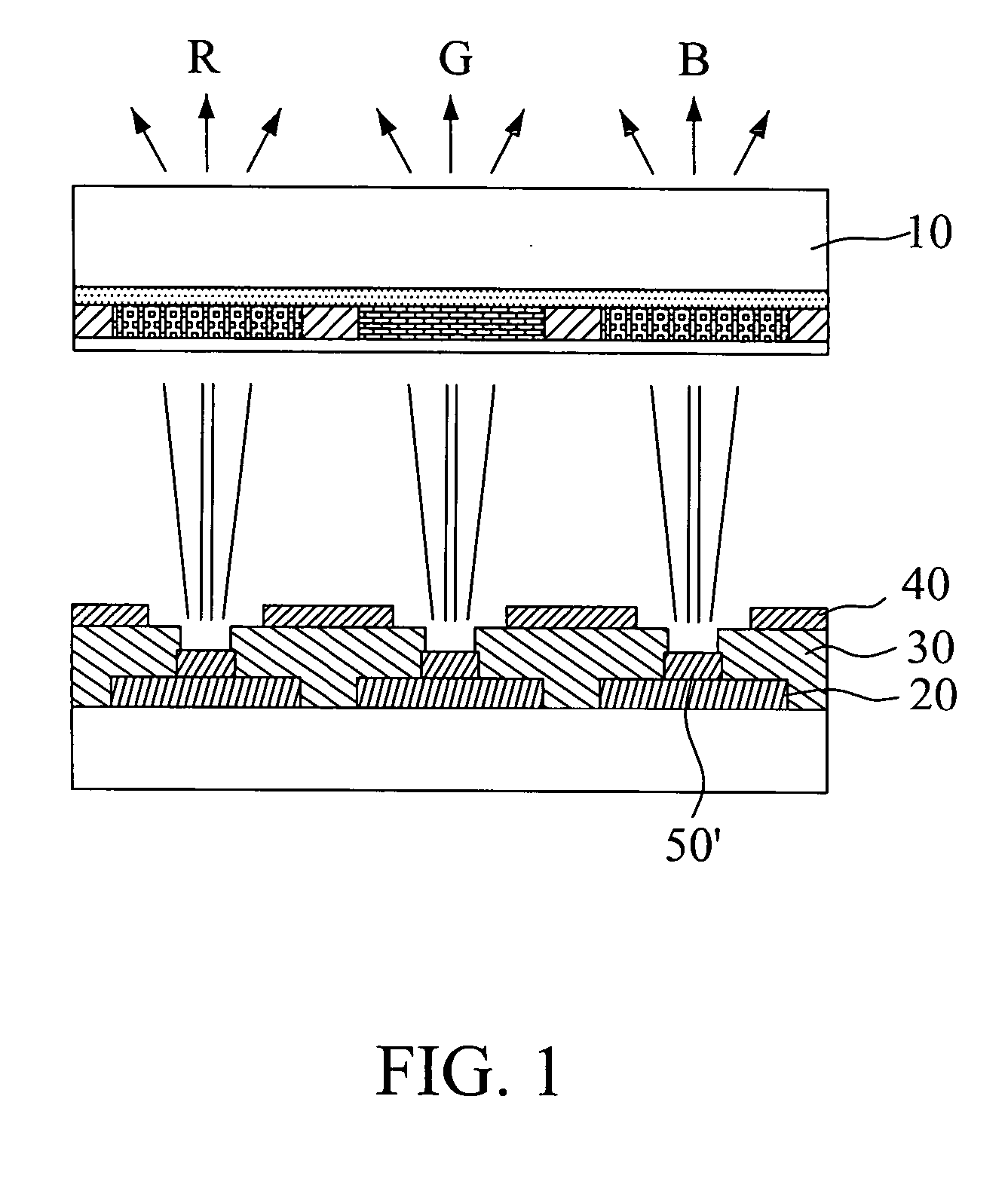
[0026] With reference to FIG. 3, a transparent or semi-transparent substrate 10 is provided, and then a thick silver layer is deposited on the substrate 10 by a thick film process and patterned to form a cathode layer 20 having a first pattern. Next, an opaque insulating layer 30 having a second pattern is formed on the substrate 10, wherein a predetermined part of the cathode layer 20 is exposed. Afterwards, a gate layer 40 having the second pattern likewise is formed on the opaque insulating layer 30. A carbon nanotube layer 50 is then coated on the entire top surface of the substrate 10. Finally, the carbon nanotube layer 50 is exposed to a light beam coming from the backside of the substrate 10 and results in a carbon nanotube field emitter 50′. Owing to the properties of the carbon nanotube layer, the carbon nanotube field emitter 50′ is mushroom in cross-sectional view, and circular in top view, as shown in FIG. 6.

embodiment 2

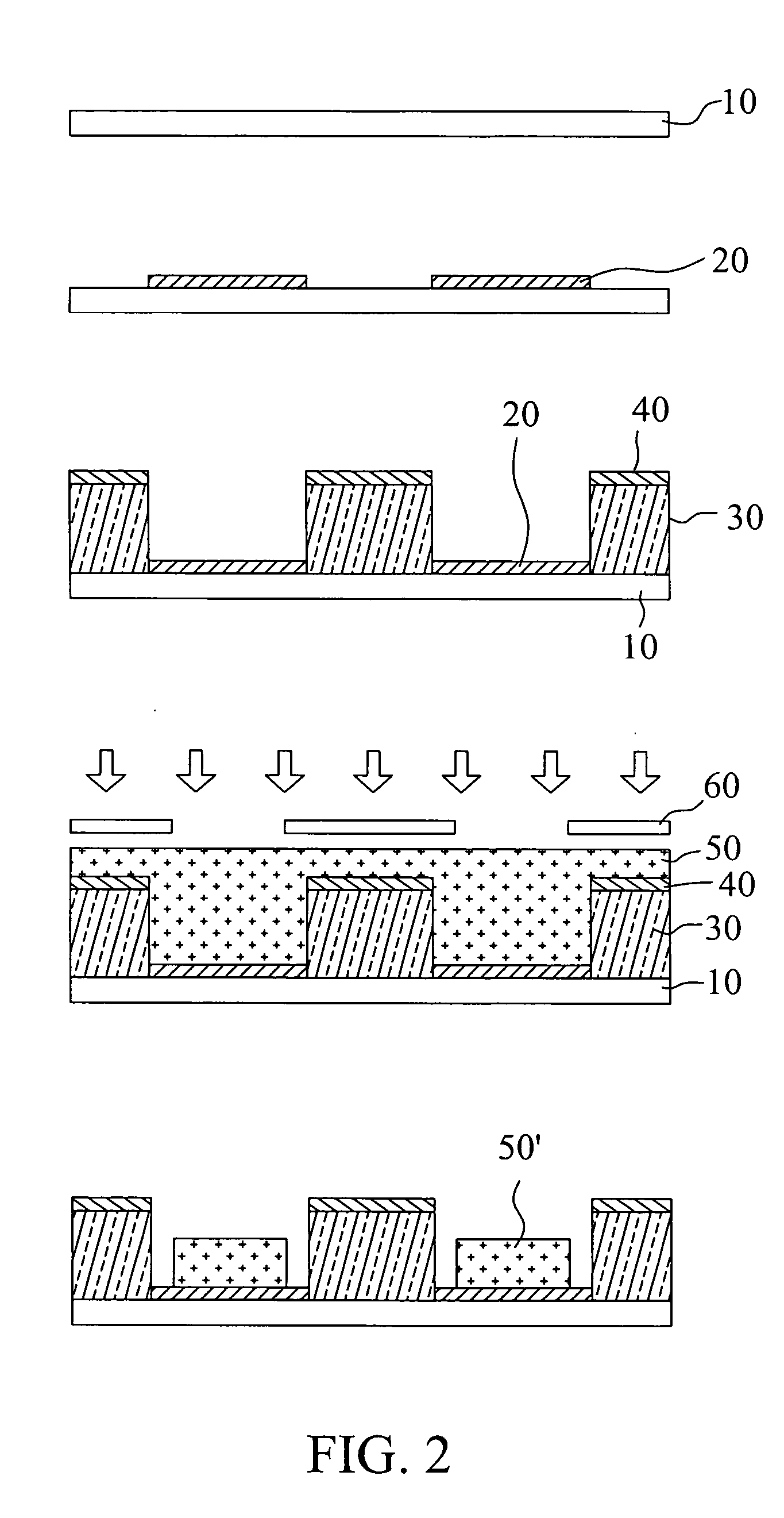
[0027] With reference to FIG. 4, a transparent or semi-transparent substrate 10 is provided, and then a thick silver layer is deposited on the substrate 10 by the thick film process and patterned to form a cathode layer 20 having a first pattern. Next, an opaque insulating layer 30 having a second pattern is formed on the substrate 10, wherein a predetermined part of the cathode layer 20 is exposed. Afterwards, a gate layer 40 having the second pattern likewise is formed on the opaque insulating layer 30. A carbon nanotube layer 50 is then coated on the entire top surface of the substrate 10. Finally, the carbon nanotube layer 50 is exposed to a light beam coming from the backside of the substrate 10 and results in a carbon nanotube field emitter 50′. Owing to the slight transparency of the silver cathode layer 20, a plurality of irregular carbon nanotube field emitters 50′ is obtained after the exposure treatment, as shown in FIG. 7.

embodiment 3

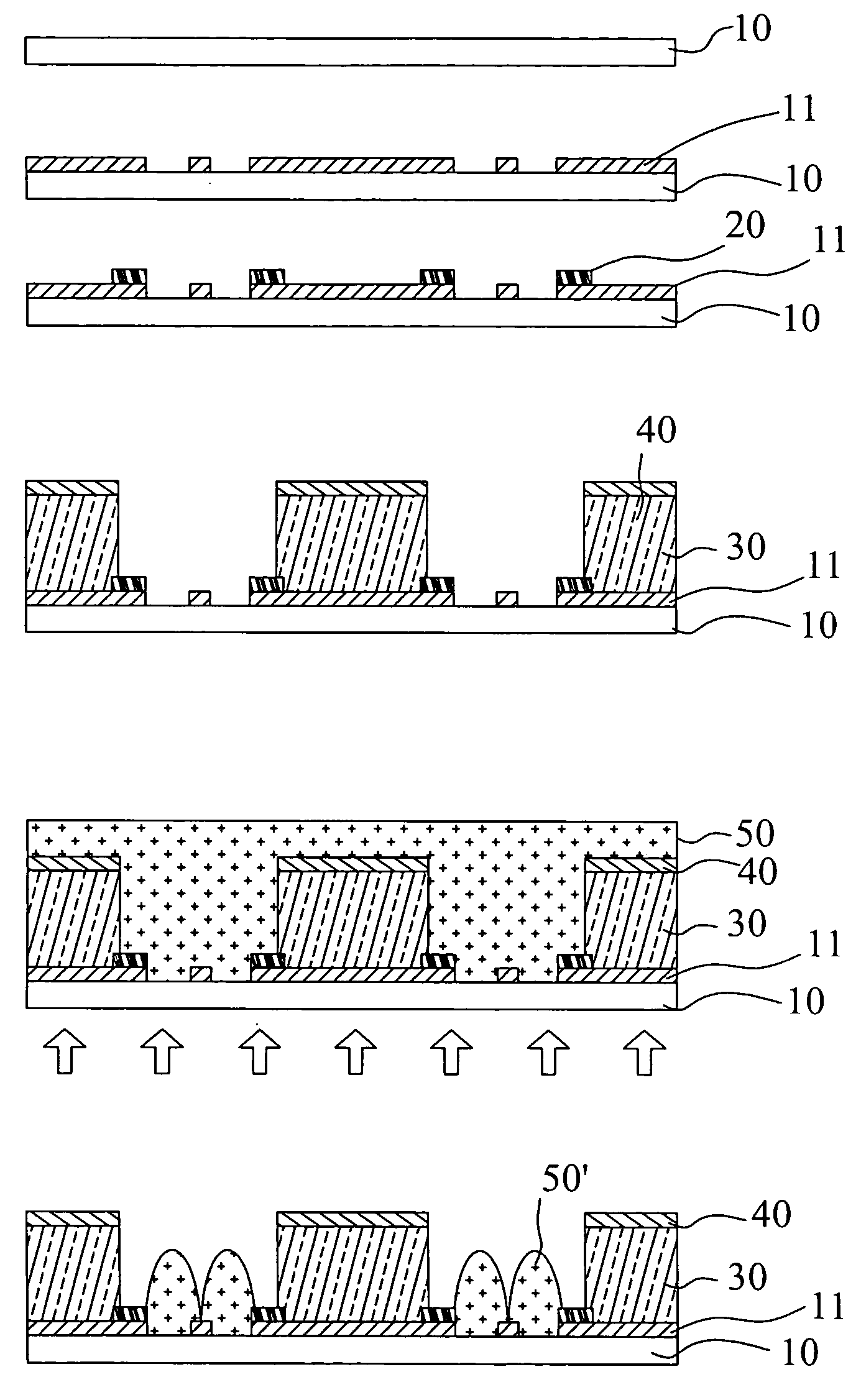
[0028] The photomask is integrated into the triode structure of the carbon nanotube field emitter array in the present embodiment, and a four-layer structure is thus formed. With reference to FIG. 5, a transparent or semi-transparent substrate 10 is provided, and then an opaque layer 11 is deposited on the substrate 10. The opaque layer 11 is patterned to form the transparent holes in a volcano shape or a donut shape. Afterwards, a silver layer is deposited and patterned to form a cathode layer 20 having a first pattern. Next, an opaque insulating layer 30 having a second pattern is formed on the substrate 10, wherein a predetermined part of the cathode layer 20 is exposed, and then a gate layer 40 having the second pattern likewise is formed on the opaque insulating layer 30. A carbon nanotube layer 50 is then coated on the entire top surface of the substrate 10. Finally, the carbon nanotube layer 50 is exposed to a light beam coming from the backside of the substrate 10 and a carb...


PUM

PropertyMeasurementUnit
transparentaaaaaaaaaa
semi-transparentaaaaaaaaaa
structureaaaaaaaaaa

Abstract

A method for fabricating a carbon nanotube field emitter array is disclosed, which has the steps of (a) providing a substrate; (b) forming a cathode layer having a first pattern on the substrate; (c) forming an opaque insulating layer having a second pattern on the substrate, wherein a predetermined part of the cathode layer is exposed; (d) forming a gate layer having the second pattern on the opaque insulating layer; (e) forming a carbon nanotube layer on the entire top surface of the substrate; and (f) exposing the carbon nanotube layer to a light beam coming from the backside of the substrate.

Description

BACKGROUND OF THE INVENTION [0001] 1. Field of the Invention [0002] The present invention relates to a carbon nanotube field emitter array and method for fabricating the same and, more particularly, to a method that integrates a photomask into the structure of the carbon nanotube field emitter array for fabricating the carbon nanotube field emitter array. [0003] 2. Description of Related Art [0004] The triode structure of a carbon nanotube field emission display (CNT-FED) is shown in FIG. 1. The triode structure has the characteristics or advantages of high electron energy, increased illumination efficiency, and low controlling voltage. In the triode structure, the anode electrode increases the energy of the electron, the cathode electrode acts as an electron emitter, and the gate electrode is responsible for drawing the electrons out of the cathode electrode. Currently, the carbon nanotube powder is first mixed with the organic materials to form a paste, which is then coated on a s...

Claims


Application Information

Patent Timeline
Patent Type & Authority Applications(United States)
IPC IPC(8): H01J29/04H01J1/304H01J9/02H01J31/12
CPCB82Y10/00H01J2201/30469H01J9/025H01J1/3042
Inventor SHEU, JYH-RONGCHAO, CHING-HSUNJIANG, LIANG-YOUCHANG, YU-YANGLEE, CHENG-CHUNG
Owner IND TECH RES INST
Why Eureka
Try Eureka