Micro-optic device and method of manufacturing same

a micro-optic and optical device technology, applied in the direction of optical elements, instruments, coatings, etc., can solve the problems of inability to have a favorable reflection response of the mirror, unevenness of the etched sidewall surface in excess of the order of 100 nm, and the difficulty of manufacturing an optical device for a micro-electromechanical system having a complicated construction, etc., to achieve rapid etching, reduce the time interval for wet etching, and achieve rapid

Inactive Publication Date: 2005-03-31
JAPAN AVIATION ELECTRONICS IND LTD
View PDF8 Cites 15 Cited by
  • Summary
  • Abstract
  • Description
  • Claims
  • Application Information

AI Technical Summary

Benefits of technology

It is an object of the present invention to provide a micro-optic device including a mirror having a smooth mirror surface which can be manufactured in a relatively reduced length of time and with a good yield, and a method of manufacturing same.
According to the present invention, the mirror surface represents either (100) plane or (111) plane, but other vertical sidewall surfaces of the optical device structure are not restricted in this manner, allowing surfaces which do not align with (100) plane or (111) plane or other crystallographic surface to remain. Accordingly, a deep etching by the anisotropic gas reactive dry etching may be applied to the single crystal silicon substrate so that the mirror surface is aligned with either (100) plane or (111) plane to form a minute structure having a complicate configuration. Subsequent to the deep etching, an etching is performed using a solution which exhibits anisotropy with respect to the crystalline orientation, whereby higher order surfaces which are subject to a rapid etching rate are quickly etched and a mirror surface becomes a crystallographic surface which is aligned with either (100) plane or (111) plane to provide a smooth mirror surface having an unevenness on the order of 10 nm or less while allowing the time interval for the wet etching to be reduced. Because sacrificial raised layers are not formed and are not required to be removed, there is no likelihood that the response may be degraded, resulting in a better yield.

Problems solved by technology

While a deep etching can be achieved by a wet etching which uses an etchant solution applied to the single crystal silicon layer, it is to be noted that this wet etching exhibits an anisotropic behaviour with respect to the crystalline orientation of the silicon, and therefore it is difficult to manufacture an optical device for a micro-electromechanical system having a complicate construction as illustrated by the optical switch shown in FIG. 1.
However, when a deep anisotropic reactive ion etching is applied to the single crystal silicon substrate 131 so that a deep vertical etched sidewall surface can be obtained, there results an unevenness which is in excess of the order of 100 nm on the etched sidewall surface.
If an etched sidewall surface having such an unevenness is used as a mirror surface for the movable mirror 115, the mirror cannot have a favorable reflection response.
If fragments of the sacrificial raised layers 138 which are separated from the substrate are jammed into these narrow spaces, the movable parts may become inoperable or there results adverse influences upon the characteristic of the micro-optic device, leading to a degraded yield.
However, with this technique, a time interval required to form an oxide film which is sufficiently thick with respect to the minute unevenness of the surface by the thermal oxidation is as long as ten hours, for example, requiring an increased manufacturing time for a micro-optic device, resulting in a high cost of the optical device.
This problem is not limited to the micro-optic switch, but a similar problem occurs when a micro-optic device including a mirror and a complicate structure other than the mirror is subject to a gas reactive, anisotropic dry etching to effect a deep etching reaction perpendicular to the surface of the substrate.

Method used


Image

  • Micro-optic device and method of manufacturing same
  • Micro-optic device and method of manufacturing same
  • Micro-optic device and method of manufacturing same

Examples


Embodiment Construction

An embodiment of the present invention applied to the micro-optic switch will now be described below with reference to the drawings. In the description to follow, it should be noted that throughout the drawings, corresponding parts are designated by like reference numbers without their repeated description.

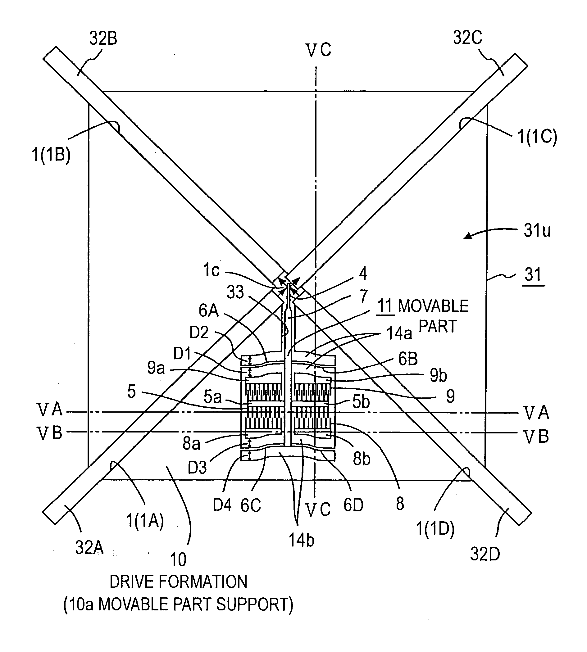
As shown in plan view in FIG. 4 and in cross sections in FIG. 5, an SOI three layer structure includes a sheet-like single crystal silicon substrate 31 having a top surface 31u in which fiber channels 1 are formed in a crisscross configuration. Four fiber channels 1A to 1D extend radially from the center 1c of an area of intersection between the crisscross fiber channels 1, and optical fibers 32A to 32D are inserted into the respective fiber channels. As shown in FIG. 6, the width of fiber channels 1A to 1D is defined so close to diameters of optical fibers 32A-32D that the fibers pressed into channels are fixed within the channels, and the end face of each optical fiber is dis...


PUM

PropertyMeasurementUnit
narrow angleaaaaaaaaaa
angleaaaaaaaaaa
thicknessaaaaaaaaaa

Abstract

A micro-optic device including a complicate structure and a movable mirror is made to be manufactured in a reduced length of time. A silicon substrate and a single crystal silicon device layer with an intermediate layer of silicon dioxide interposed therebetween defines a substrate on which a layer of mask material is formed and is patterned to form a mask having the same pattern as the configuration of the intended optical device as viewed in plan view. A surface which is to be constructed as a mirror surface is chosen to be in a plane of the silicon crystal. Using the mask, the device layer is vertically etched by a reactive ion dry etching until the intermediate layer is exposed. Subsequently, using KOH solution, a wet etching which is anisotropic to the crystallographic orientation is performed with an etching rate which is on the order of 0.1 μm / min for a time interval on the order of ten minutes is performed to convert the sidewall surface of the mirror into a smooth crystallographic surface. Subsequently, the intermediate layer is selectively subject to a wet etching to remove the intermediate layer only in an area located below the movable part of the optical device.

Description

BACKGROUND ART The present invention relates to a micro-optic device including a mirror and a complicate structure fabricated by a deep dry etching technique such as a micro-optic device which is capable of light path switching and light intensity adjustment utilizing a mirror, and to a method of manufacturing such a device. An optical switch has been proposed in which a technique such as a semiconductor anisotropic dry etching is used to form elements including a mirror, a hinge, an actuator and a light guide on a substrate and which has the function of switching a light path by insertion into and extraction from the light guide of the mirror. To give a specific example, the structure of an MEMS (Micro-Electro-Mechanical System) optical switch disclosed in U.S. Pat. No. 6,315,462, issued Nov. 13, 2001, is shown in FIG. 1. Formed in a sheet-like substrate 111 are four fiber channels 112a to 112d in a crisscross configuration. One of four areas which is defined by the fiber chann...

Claims


Application Information

Patent Timeline
Patent Type & Authority Applications(United States)
IPC IPC(8): B81B3/00B81C1/00G02B6/35G02B26/08
CPCB81B3/0083B81B2201/045B81C1/00182G02B6/122G02B6/136G02B26/0841G02B6/3518G02B6/3546G02B6/357G02B6/3584G02B6/3596G02B6/3514
Inventor KATO, YOSHICHIKAYOSHIDA, SATOSHIMORI, KEIICHIKONDOU, KENJIHAMADA, YOSHIHIKOIMAKI, OSAMU
Owner JAPAN AVIATION ELECTRONICS IND LTD
Why Eureka
Try Eureka