Etching solution, etching method and method for manufacturing semiconductor device

a semiconductor device and etching solution technology, applied in the direction of electrical equipment, surface treatment compositions, chemical instruments and processes, etc., can solve the problems of leakage current generation, achieve greater ionization tendency, prevent metal compounds, and increase ionization tendency

Inactive Publication Date: 2005-03-31
SONY CORP
View PDF1 Cites 11 Cited by
  • Summary
  • Abstract
  • Description
  • Claims
  • Application Information

AI Technical Summary

Benefits of technology

[0007] Thus, one of the problems to be solved by the invention is to prevent interstitial corrosion of copper on etching of the barrier layer. Another problem is to prevent erosion in a region where the copper wiring is densely arranged, thereby permitting groove wirings of 0.1 μm and subsequent generations to be more miniaturized.
[0025] With the manufacturing method using a polishing slurry to which an anticorrosive capable of preventing copper from being corroded in the course of polishing during a wiring step and rendering the copper surface hydrophobic is added, when tungsten, a tungsten compound, tantalum, a tantalum compound, titanium or a titanium compound is used as a barrier layer for the formation of a groove wiring of copper, the following advantages are obtained. The corrosion of copper can be suppressed when copper is polished (for example, by chemical mechanical polishing), and erosion is prevented from occurring in a region of high copper wiring density because of the hydrophobicity on the surface of the copper wiring. Especially, when tungsten, tungsten nitride, titanium or the like whose potential difference from copper is as great as 300 mV to 400 mV and is greater in ionization tendency than copper is used, the corrosion of copper can be advantageously suppressed upon polishing of copper (e.g. by chemical mechanical polishing). This enables one to adopt, as a barrier layer, a metal film or metal compound film that can be formed according to a CVD method or an ALD method ensuring excellent coverage on use as a barrier metal for copper wiring of a groove wiring structure. Thus, an advantage is obtained in that the method is responsible for the miniaturization of groove wirings of copper for the 0.1 μm and subsequent generations.

Problems solved by technology

This thinly left barrier layer serves as an insulation failure layer, thereby causing a leak current to be generated.
Another problem is to prevent erosion in a region where the copper wiring is densely arranged, thereby permitting groove wirings of 0.1 μm and subsequent generations to be more miniaturized.

Method used


Image

  • Etching solution, etching method and method for manufacturing semiconductor device
  • Etching solution, etching method and method for manufacturing semiconductor device
  • Etching solution, etching method and method for manufacturing semiconductor device

Examples


example 1

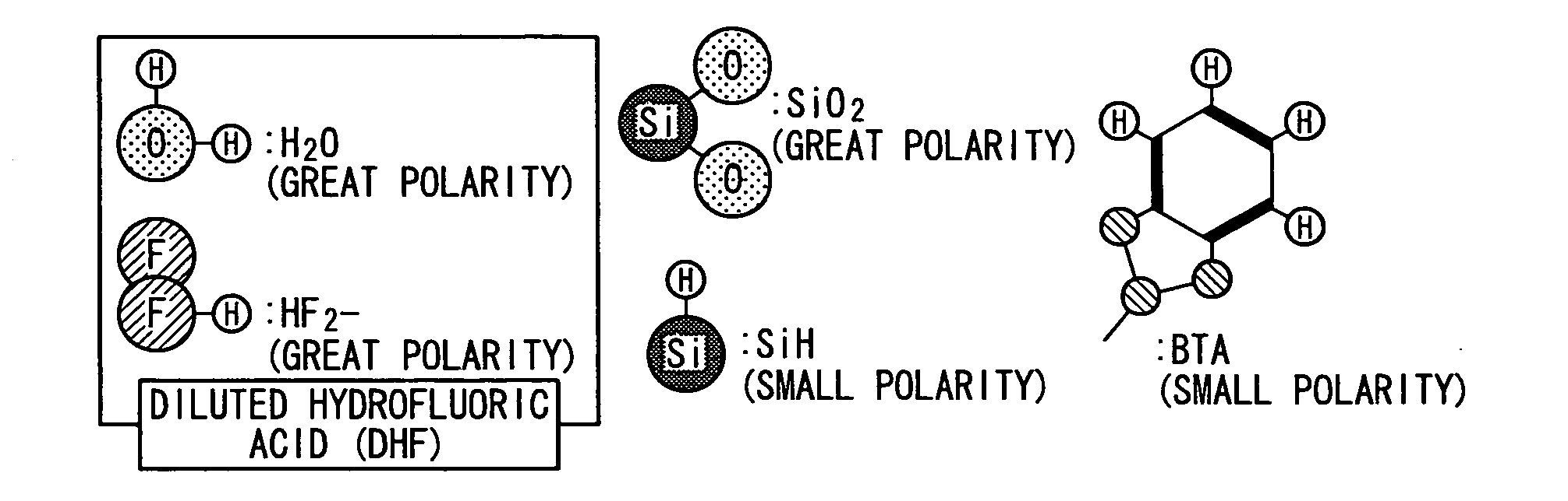
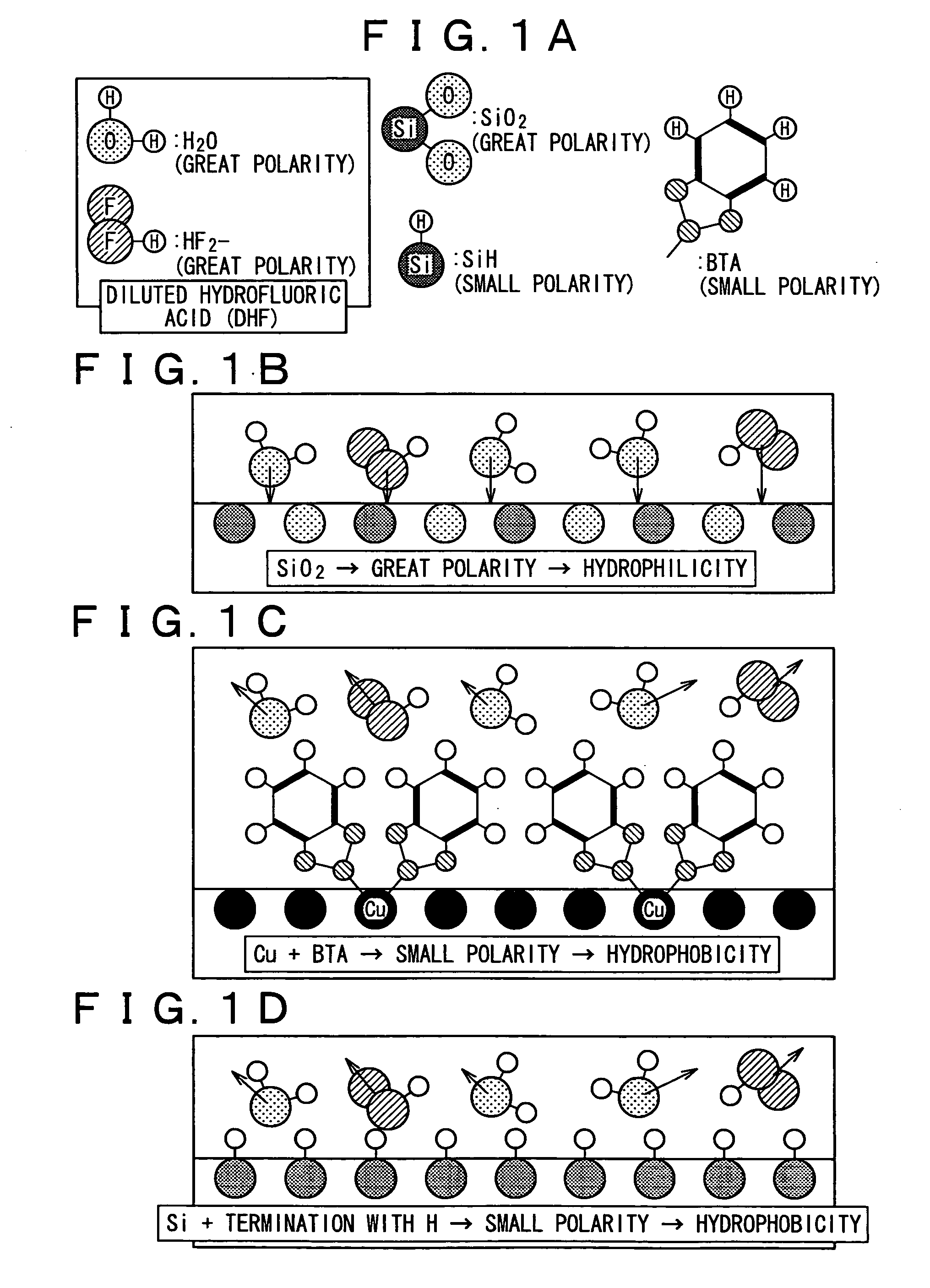
[0040] The etching solution of the invention is one which contains an anticorrosive for copper in a hydrofluoric acid aqueous solution. The hydrofluoric acid aqueous solution is, for example, a hydrofluoric acid aqueous solution containing 0.1% to 10%, preferably 0.1% to 2.0%, in which at least an anticorrosive for copper should be contained. The anticorrosive for copper is favorably contained in an amount, for example, of about 500 ppm.

[0041] The anticorrosive should preferably have a molecule size of not larger than 10 nm, for which at least one of a benzotriazole, a carboxylbenzotriazole, a methylbenzotriazole, a benzotriazole butyl ester, a silver benzotriazole and a chlorobenzotriazole can be used. As a matter of course, the anticorrosives may be used in combination. The size of the molecules is approximately at 1 nm. Since an anticorrosive for copper whose size of molecule is not larger than 10 nm is used, the copper surface can be protected such that if a narrow interstice (...

example 2

[0055] Next, the etching methods of the invention are described below.

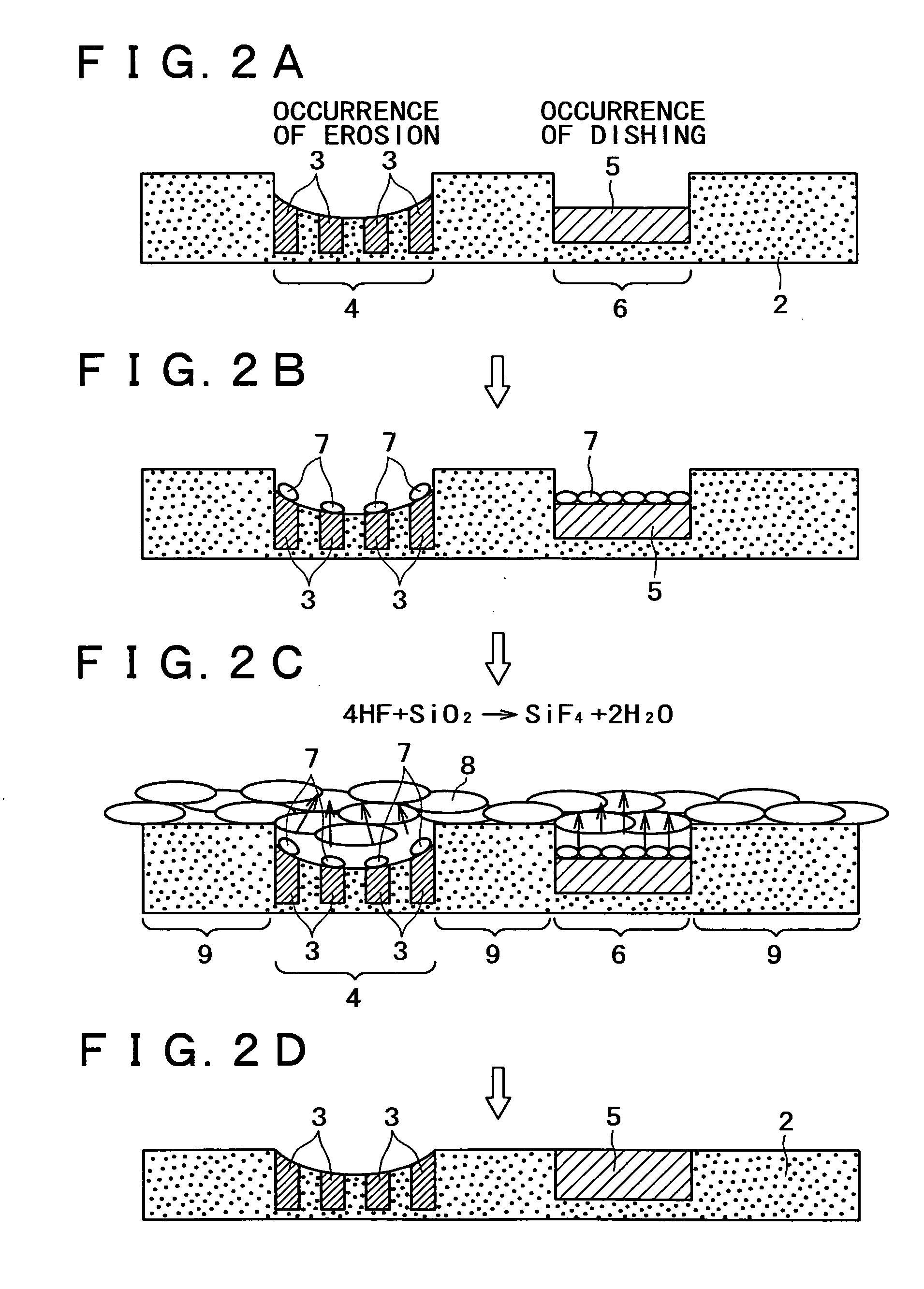
[0056] A first etching method of the invention is one which includes etching a surface layer of an insulating film having copper and a metal or metal compound, which is greater in ionization tendency than copper, exposed on the surface thereof and also having the metal, which is greater in ionization tendency than copper, or metal compound left thereof. Initially, an anticorrosive for copper is applied onto the copper surface to form a protective film. For the anticorrosive for copper, at least one of a benzotriazole, a carboxylbenzotriazole, a methylbenzotriazole, a benzotriazole butyl ester, a silver benzotriazole, and a chlorobenzotriazole can be used. Next, a hydrofluoric acid aqueous solution is used to remove the surface layer of the insulating film in which the metal, which is greater in ionization tendency than copper, or metal compound is left. In this way, the metal, which is greater in ionization tende...

example 3

[0064] A second etching method of the invention is one wherein using such a hydrofluoric acid aqueous solution containing an anticorrosive for copper as set out hereinbefore, the surface layer of the insulating film on which copper and the metal, which is greater in ionization tendency than copper, or metal compound are both exposed and the metal, which is greater in ionization tendency than copper, or metal compound is left is etched to remove the metal, which is greater in ionization tendency than copper, or metal compound left on the insulating film.

[0065] The etching solution used in the second etching method is prepared in the following way.

[0066] In a first preparation method, an etching solution is obtained by adding, to a hydrofluoric acid aqueous solution (having a concentration of 0.1 vol % to 10 vol %, preferably 0.1 vol % to 2.0 vol %), 10 ppm to 500 ppm of such an anticorrosive for copper as illustrated hereinbefore and is used for etching.

[0067] In a second preparat...


PUM

PropertyMeasurementUnit
molecule sizeaaaaaaaaaa
thicknessaaaaaaaaaa
sizeaaaaaaaaaa

Abstract

An etching solution includes an anticorrosive for copper or a benzotriazole based anticorrosive in a hydrofluoric acid aqueous solution. An etching method makes use of the etching solution set out above. Moreover, a method for manufacturing a semiconductor device which should include the step of removing copper by the etching method. The method includes the steps of forming copper through a barrier layer made of a metal or metal compound, which is greater in ionization tendency than copper, so as to bury a wiring groove formed in an insulating film with the copper, followed by polishing additional copper and barrier layer formed on the insulating film, and etching a surface layer of the insulating film by use of the etching solution to remove an insulating defective layer made mainly of the barrier layer on the insulating film along with the surface layer of the insulating film.

Description

BACKGROUND OF THE INVENTION [0001] This invention relates to an etching solution, an etching method and a method for manufacturing a semiconductor device. More particularly, the invention relates to an etching solution adapted for use in etching at the time of forming copper wiring, an etching method using the etching solution, and a method for manufacturing a semiconductor device using the etching method. [0002] Copper wirings having a conventional groove wiring structure are formed in the following way. More particularly, as shown in FIG. 11A, copper 116 made of a copper seed layer 114 and a copper plated layer 115 is buried in a wiring groove 112 formed in an insulating film 111 via a barrier layer 113. Thereafter, additional copper 116 on the insulating film 111 is removed by chemical mechanical polishing (hereinafter referred to simply as CMP). In addition, an additional barrier layer 113 over the insulating film 111 is also removed by CMP making use of a polishing slurry for a...

Claims


Application Information

Patent Timeline
Patent Type & Authority Applications(United States)
IPC IPC(8): H01L21/3205C09K13/06C09K13/08C23F1/26H01L21/306H01L21/3105H01L21/321H01L21/768
CPCC09K13/06C09K13/08H01L21/7684H01L21/31053H01L21/3212C23F1/26
Inventor OHTORII, HIIZUTAI, KAORIHORIKOSHI, HIROSHIKOMAI, NAOKISATO, SHUZO
Owner SONY CORP
Why Eureka
Try Eureka