Semiconductor device and method for manufacturing the same
a semiconductor and semiconductor technology, applied in the direction of semiconductor devices, semiconductor/solid-state device details, electrical apparatus, etc., can solve the problems of mos transistor performance being remarkably degraded, fine transistors not being able to be formed, and damage to the silicon substrate b>101/b>, so as to prevent damage to the semiconductor substrate without excessively complicating the manufacturing process
- Summary
- Abstract
- Description
- Claims
- Application Information
AI Technical Summary
Benefits of technology
Problems solved by technology
Method used
Image
Examples
first embodiment
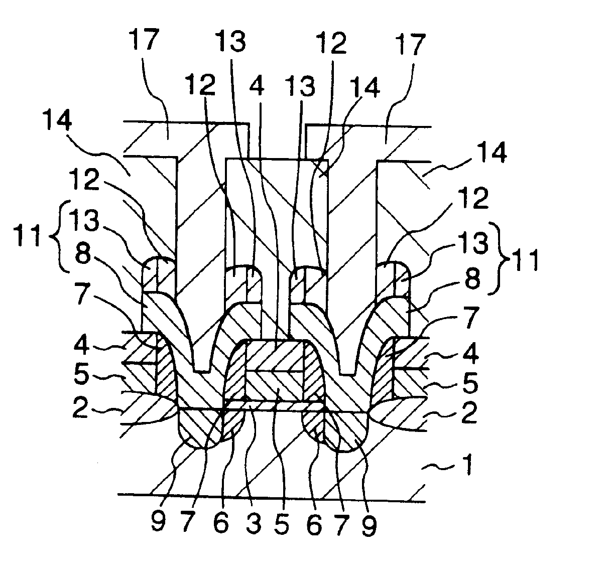
[0037] Referring first to FIGS. 3A to 3I, there are illustrated cross sectional views showing a semiconductor device according to the present invention and a method for manufacturing the same in order of process.
[0038] Firstly, as shown in FIG. 3A, a field oxide film 2 with about 400 nm thickness is formed in a region to be an isolation region of a P-type semiconductor silicon substrate 1 containing boron and having resistivity in the range of 1 to 12 Ω-cm by the well-known LOCOS method. Thereafter, a gate oxide film 3 with a thickness of 10 to 20 nm, or so, is formed on an active region, which is surrounded by the field oxide film 2, by the thermal oxidation method.
[0039] Then, after a polycrystalline silicon film about 100 nm thick containing phosphorus or arsenic of 2×10²⁰ to 6×10²⁰ atoms / cm3 is formed by the CVD method, a silicon oxide film 4 about 200 nm thick is formed on that polycrystalline silicon film by the CVD method. Thereafter, a photo resist film (not shown) is appli...
second embodiment
[0059] Next, a description will be given with respect to a semiconductor device according to the present invention and a method for manufacturing the same with reference to FIGS. 6A to 6E.
[0060] In the manufacturing process of the present embodiment, by carrying out the same process as that shown in FIGS. 3A to 3E in the first embodiment of the present invention, there is obtained a structure, as shown in FIG. 6A, having a pattern in which the silicon oxide film (the first mask layer) 12 is separated into portions, located on both sides of the gate electrode 5, with the width of the gate length.
[0061] Next, as shown in FIG. 6B, a silicon oxide film (a second mask layer) 51 about 200 nm thick is formed on the whole surface of the silicon substrate 1 by the CVD method.
[0062] Next, as shown in FIG. 6C, the silicon oxide film 51 is selectively etched away by the anisotropic dry etching so as to be left only on both side faces of the silicon oxide film 12.
[0063] Subsequently, the poly...
PUM
 Abstract
Description
Claims
Application Information
 - R&D
- Intellectual Property
- Life Sciences
- Materials
- Tech Scout
- Unparalleled Data Quality
- Higher Quality Content
- 60% Fewer Hallucinations
Browse by: Latest US Patents, China's latest patents, Technical Efficacy Thesaurus, Application Domain, Technology Topic, Popular Technical Reports.
© 2025 PatSnap. All rights reserved.Legal|Privacy policy|Modern Slavery Act Transparency Statement|Sitemap|About US| Contact US: help@patsnap.com


