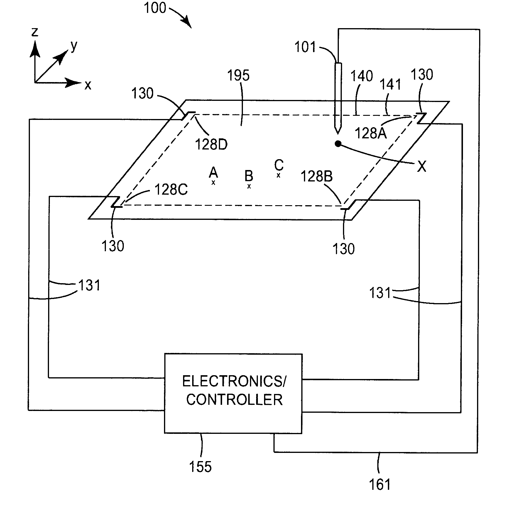
Touch input sensing device

a sensing device and input technology, applied in the field of sensing devices, can solve the problems of reducing the touch accuracy of the sensor or even rendering the device nonfunctional, increasing manufacturing costs, and not sufficiently protecting the conductive film, so as to achieve the effect of low temperature processing, increased resistance to scratches, and low cos

Inactive Publication Date: 2005-04-07
3M INNOVATIVE PROPERTIES CO
View PDF18 Cites 173 Cited by
  • Summary
  • Abstract
  • Description
  • Claims
  • Application Information

AI Technical Summary

Benefits of technology

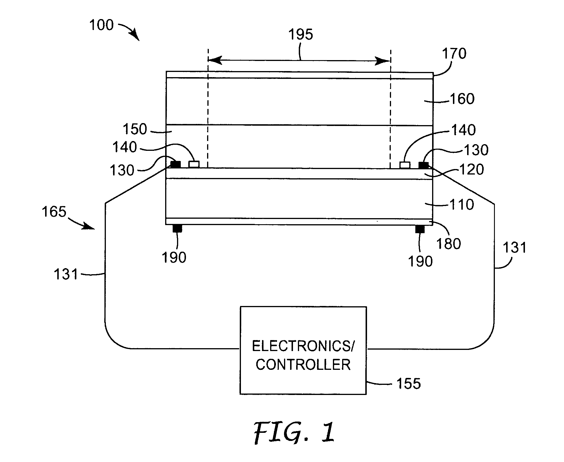
[0035] A particular advantage of the present invention is that glass layer 160 is sufficiently thin to allow detection of a signal induced by capacitive coupling between a conductive touch implement and the conductive film 120. At the same time, according to the present invention, glass layer 160 is thick enough to make the layer self-supporting and processable. Furthermore, glass layer 160 is thick enough so that abrasion due to, for example, normal use results in fewer or no cosmetic defects such as discoloration that would normally occur when the thickness of layer 160 is on the order of a few wavelengths. In addition, glass layer 160 is thick enough to protect the conductive film 120 from damage, such as a deep scratch in the glass layer, which may result from a user's fingernail, a coin, a pen, or any sharp touch input applied to the touch sensitive area 195.
[0036] Another particular advantage of the present invention is that layer 160 includes glass. A layer similar to layer 160 in thickness, but made of organic materials such as polycarbonate, acrylic, polyethylene terephthalate (PET), polyvinyl chloride (PVC), polysulfone, and the like, would be much softer than glass and therefor, more susceptible to scratches. For example, according to a pencil hardness test (see ASTM D 3363, Test Method for Film Hardness by Pencil Test) PET has a pencil hardness of about 1H, whereas glass has a much higher hardness of about 6H. According to the present invention, layer 160 includes glass to protect conductive layer 120 from damage, and is preferably flexible to make it more processable. A flexible layer 160 often means a thin layer 160. Therefore, according to one aspect of the present invention, flexible layer 160 is sufficiently thin so that signals induced by capacitive coupling between a conductive touch implement and a conductive film 120 are sufficiently large to make the induced signal detectable and differentiable from background noise so that the touch location can be adequately determined.
[0037] Another advantage of the present invention is low temperature processing. Conventional capacitive touch sensors typically use a thin sol-gel based silica coating to protect the conductive film. The sol-gel coating can often require a high temperature curing or sintering step, sometimes referred to as firing, that can exceed 500° C. In contrast, according to one aspect of the present invention, the optional bonding layer 150 can be used to bond the thin glass layer 160 to the conductive film 120 at low temperatures, for example, at approximately room temperature. Low temperature processing is particularly advantageous where the conductive film 120 cannot withstand high temperature processing. For example, conductive organic layers, such as an intrinsically conductive polymer, typically cannot withstand high temperature processing. According to one aspect of the present invention, the optional bonding layer 150 can be dried and / or cured at low temperatures. For example, the bonding layer can be cured by exposure to radiation, such as Ultra Violet (UV) radiation. In the case of exposure to UV radiation, it may be advantageous for the bonding layer to include UV absorbers to protect the conductive film 120 from UV radiation. The bonding layer can also be cured at other wavelengths or wavelength ranges, such as blue or green. In one aspect of the invention, the bonding layer can be cured by exposure to gamma radiation. In another aspect of the present invention, the bonding layer can be thermally cured. The curing temperatures can be well below temperatures that could adversely affect other layers in the touch sensor 100. In general, the bonding layer may be solidified and / or cured using any drying and / or curing technique. It will be appreciated that although it may be advantageous for the bonding layer to be solidified and / or cured at low temperatures, the bonding layer can be processed at high temperatures. For example, the bonding layer 150 can include a sol-gel and may be cured by a firing step.
[0038] An advantage of using the optional bonding layer 150 can be improved touch sensor impact and shatter resistance. Bonding layer 150 can provide adhesive support for glass layer 160 across the touch sensor area, for example, across the touch sensitive area 195. In the event glass layer 160 breaks, the broken fragments can remain adhered to other components in touch sensor 100, such as substrate 110. Increased shatter resistance can permit use of a thinner glass layer 160.
[0039] The present invention is particularly advantageous in a capacitive touch sensor or a capacitive touch display system that includes one or more layers that are sensitive to environmental factors such as oxygen and moisture, especially at elevated temperatures. Generally, permeability coefficient of organic layers can be quite high. For example, permeability coefficient of poly-methyl-methacrylate is 0.116×10⁻¹³ (cm3×cm) / (cm2×s×Pa) for oxygen at 34° C. and 480×10−13 (cm3×cm) / (cm2×s×Pa) for water at 23° C. (see, for example, Polymer Handbook, 4th Edition, J. Brandrup, E. I. Immergut, and E. A. Grulke, Publisher: John Wiley, & Sons, Inc., page VI / 548). In sharp contrast, the permeability coefficient of a glass layer 160 is effectively zero for any permeant such as oxygen and water. As such, layer 160 can be utilized to effectively protect environmentally sensitive layers from environmental factors such as oxygen and moisture. One such environmentally sensitive layer is a conductive polymer film. Other environmentally sensitive layers include, for example, active layers used in an OLED device.
[0040] Substrate 110 can be electrically insulating. Substrate 110 may be rigid or flexible. Substrate 110 may be optically opaque or transmissive. The substrate may be polymeric or any type of glass. For example, the substrate may be float glass, or it may be made of organic materials such as polycarbonate, acrylic, polyethylene terephthalate (PET), polyvinyl chloride (PVC), polysulfone, and the like. Substrate 110 may include a metal, in which case, the substrate can also be used as conductive film 120.

Problems solved by technology

A touch implement can scratch or otherwise damage a touch sensor, thereby reducing the touch accuracy of the sensor or even rendering the device nonfunctional.
The thin dielectric coating, however, is very thin, typically no more than one micron in thickness and therefore, may not sufficiently protect the conductive film from damage that can be caused by, for example, a sharp touch implement.
A thicker dielectric coating can increase manufacturing cost and can generally reduce the coating quality by introducing stress-related cracks and cosmetic defects in the coating.
Furthermore, abrasion of the thin dielectric coating under normal use can result in thickness variation in the thin dielectric coating.
Such variation can affect touch accuracy and result in undesirable visible cosmetic defects.

Method used


Image

  • Touch input sensing device
  • Touch input sensing device
  • Touch input sensing device

Examples


example 1

[0065] A touch sensor according to one embodiment of the present invention was assembled as follows.

[0066] A 3 mm thick square soda lime glass substrate was dip coated in a solution containing an organic conductive material available from Bayer Company under the trade designation Baytron P. The solution further included ethylene glycol and an epoxysilane coupling agent. The solution was diluted with isopropyl alcohol. The glass substrate was coated on both sides from the dipping process. The coated glass substrate was dried and cured at 85° C. for 6 minutes, resulting in conductive polymer films being formed on both sides of the glass substrate.

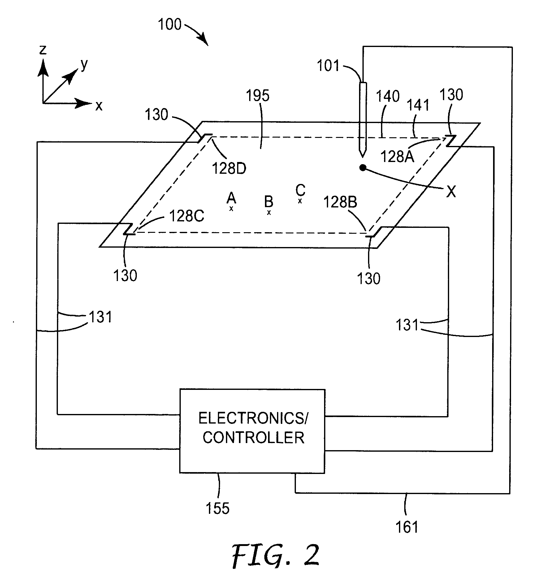
[0067] Next, a linearization pattern was screen printed along the perimeter of one side of the panel using a carbon-loaded conductive ink. The printed substrate was cured at 130° C. for 6 minutes.

[0068] Next, conductive leads were connected to the four corners of the linearization pattern using a conductive epoxy. The assembly was cured at...

example 2

[0072] A touch sensor according to one embodiment of the present invention was prepared similar to Example 1, except that a 0.4 mm thick rectangular soda lime glass substrate was used for the dip coating. The completed assembly was activated using a controller EX II. A finger draw test resulted in a linearity better than 1%.

example 3

[0073] A touch sensor according to one embodiment of the present invention was assembled as follows.

[0074] A linearization pattern was screen printed along the perimeter of one side of a 3 mm thick rectangular soda lime glass substrate that was coated, on the same side, with a 1500 ohms per square TAO. The conductive ink used to print the linearization pattern was from DuPont Company under the trade designation 7713. The printed substrate was cured at 500° C. for 15 minutes.

[0075] Next, conductive leads were connected to the four corners of the linearization pattern similar to Example 1.

[0076] Next, a 0.4 mm thick square soda lime glass was bonded to the side of the panel that was printed with the linearization pattern. The bonding was accomplished using an optical adhesive from Norland Corporation under the trade designation NOA 68. The adhesive was cured using ultra violet radiation.

[0077] Next, the completed assembly was activated using a controller EX II connected to the con...


PUM


Abstract

A touch sensor and a method of sensing are disclosed. The touch sensor includes a self-supporting flexible glass layer disposed on a conductive film. The touch sensor further includes electrical circuitry configured to detect a signal induced by capacitive coupling between the conductive film and a touch input applied to the flexible glass layer.

Description

FIELD OF THE INVENTION [0001] This invention generally relates to sensing devices. The invention is particularly applicable to capacitive sensing devices. BACKGROUND [0002] Touch screens allow a user to conveniently interface with an electronic display system by reducing or eliminating the need for a keyboard. For example, a user can carry out a complicated sequence of instructions by simply touching the screen at a location identified by a pre-programmed icon. The on-screen menu may be changed by re-programming the supporting software according to the application. As another example, a touch screen may allow a user to transfer text or drawing to an electronic display device by directly writing or drawing onto the touch screen. [0003] Resistive and capacitive are two common touch sensing methods employed to detect the location of a touch input. Resistive technology typically incorporates two transparent conductive films as part of an electronic circuit that detects the location of a...

Claims


Application Information

Patent Timeline
Patent Type & Authority Applications(United States)
IPC IPC(8): G06F3/033G06F3/044G06F3/048
CPCG06F3/044G06F3/0443G06F3/0416
Inventor RICHTER, PAUL J.CAIRNS, DARRAN R.BOTTARI, FRANK J.
Owner 3M INNOVATIVE PROPERTIES CO
Why Eureka
Try Eureka