

Organic electroluminescent device
a technology of electroluminescent devices and organic materials, which is applied in the direction of discharge tube luminescnet screens, natural mineral layered products, etc., can solve the problems of high efficiency, inability to achieve white color, and inability to obtain light with a high luminance, etc., and achieve high efficiency
- Summary
- Abstract
- Description
- Claims
- Application Information
AI Technical Summary
Benefits of technology
Problems solved by technology
Method used
Image

Examples
first embodiment
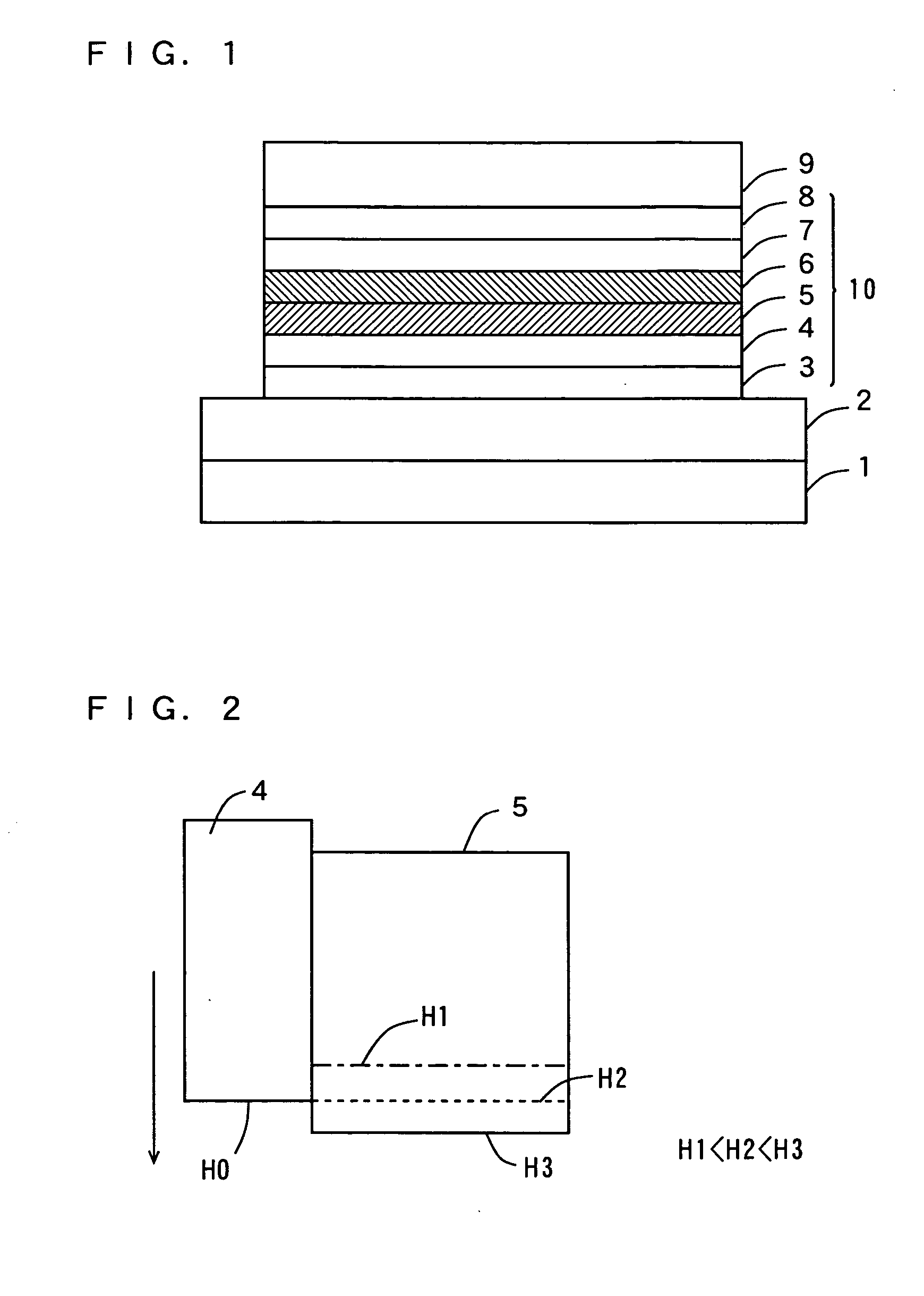
[0054]FIG. 1 is a schematic sectional view showing an organic EL device according to a first embodiment of the present invention.
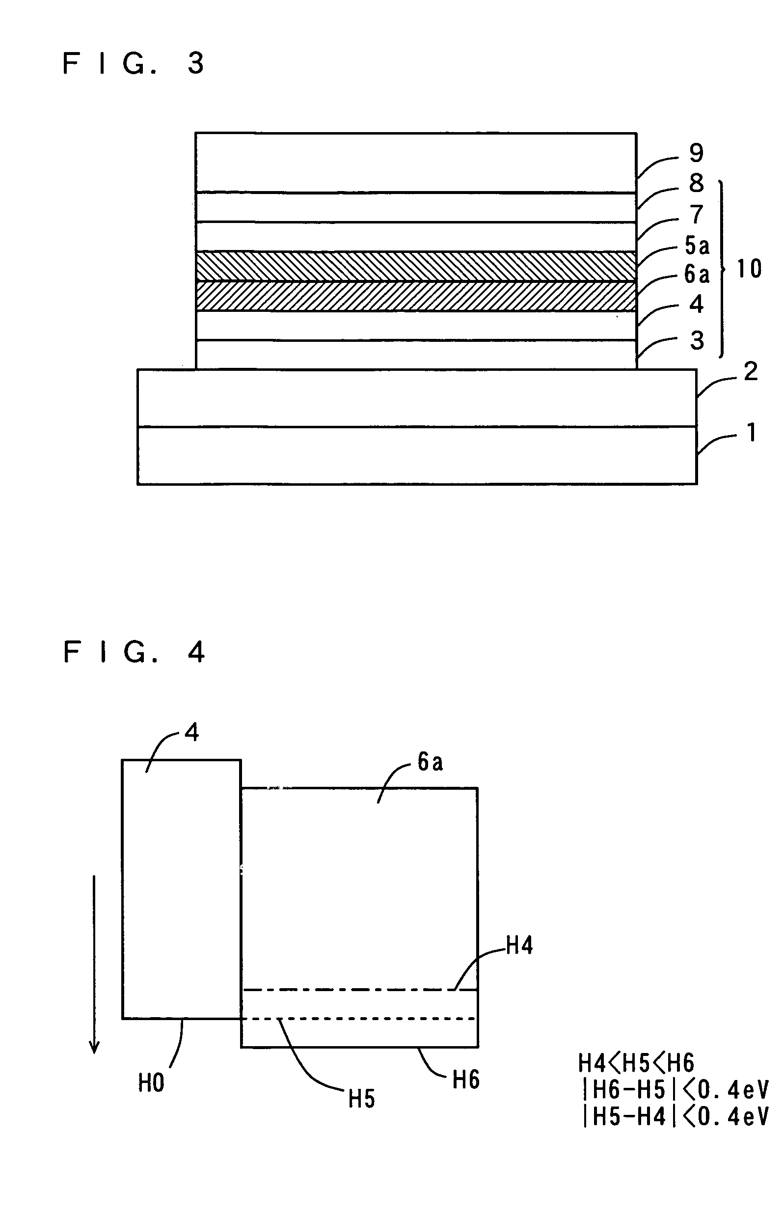
[0055] In fabrication of an organic EL device 100 shown in FIG. 1, an anode 2 composed of In2O3—SnO2 (ITO) is previously formed on a glass substrate 1, and a hole injection layer 3, a hole transport layer 4, a blue light emitting layer 5, an orange light emitting layer 6, an electron transport layer 7, and an electron injection layer 8 are formed in this order by a vapor deposition at a vacuum in the 10−4 Pa order, to form an organic thin film layer 10. Further, a cathode 9 composed of an alloy of magnesium and indium (Mg:In) is formed on the organic thin film layer 10.
[0056] The hole transport layer 4 is composed of an amine-based material such as N,N′-Di(naphthalene-1-yl)-N,N′-diphenyl-benzidine (hereinafter referred to as NPB) having a molecular structure expressed by the following formula (D1), 4,4′4″-Tris(N-(2-naphthyl)-N-phenyl-amino)-triphenylamin...
second embodiment
[0098]FIG. 3 is a schematic sectional view showing an organic EL device according to a second embodiment.
[0099] The organic EL device shown in FIG. 3 differs from the organic EL device shown in FIG. 1 in that a blue light emitting layer 5a and an orange light emitting layer 6a shown in FIG. 3 are formed in an order reverse to the blue light emitting layer 5 and the orange light emitting layer 6 shown in FIG. 1.
[0100] The orange light emitting layer 6a has a structure in which the assisting dopant is doped into the host material composing the orange light emitting layer 6 shown in FIG. 1. An example of an assisting dopant to be doped into a host material composing the orange light emitting layer 6a is NPB, Rubrene, or Ir(ppy) used for a hole transport layer 4.
[0101] In the orange light emitting layer 6a, the volume ratio of a luminescent dopant to the host material is approximately 6.5%, and the volume ratio of the assisting dopant thereto is 0% to 40%, for example. The volume rat...
##ventive example 1
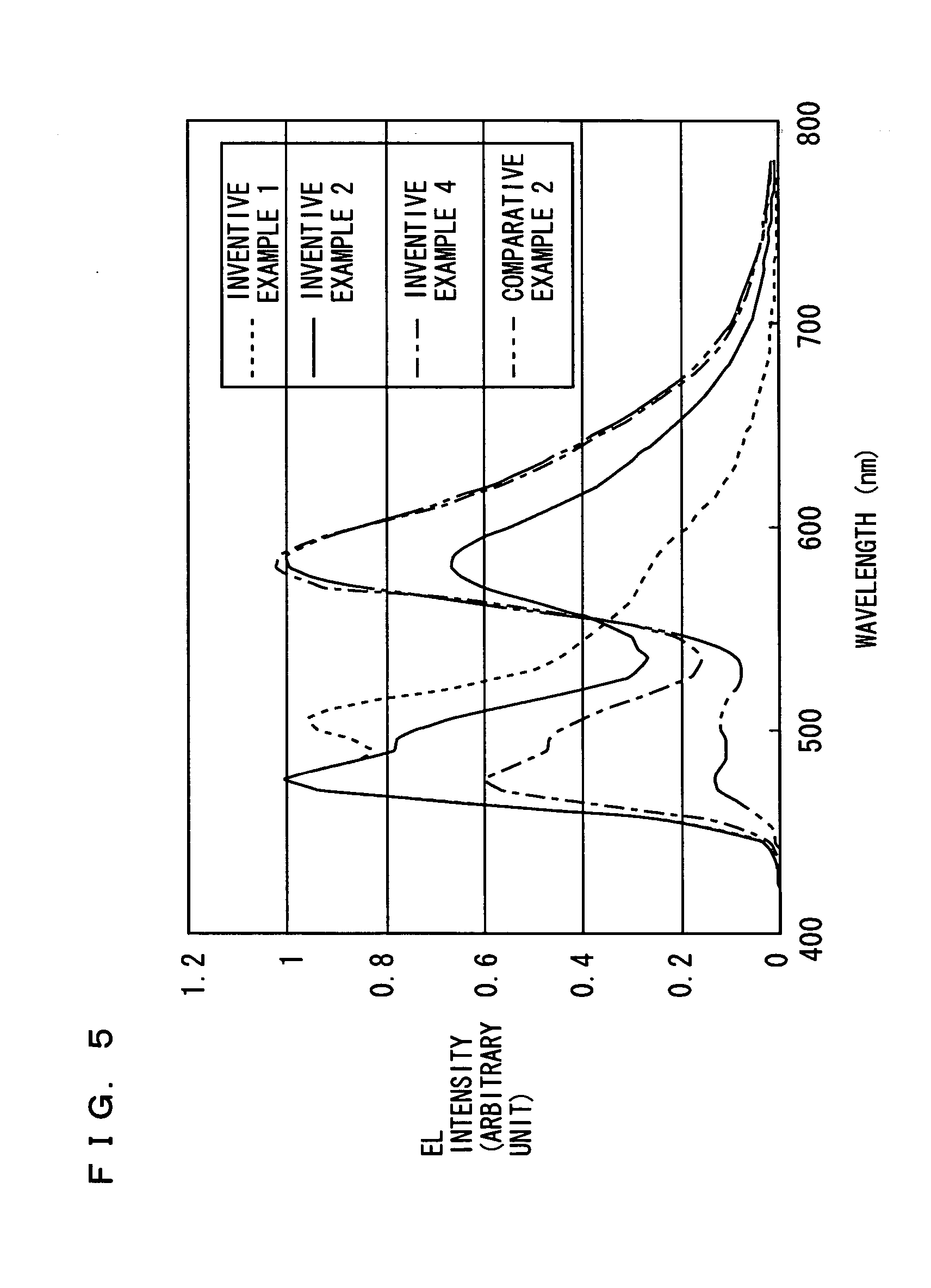
Inventive Example 1
[0113] In the inventive example 1, the organic EL device having the structure A was prepared. First, the anode 2 was formed on the glass substrate 1 by 80 nm sputtering. The glass substrate 1 having the anode 2 formed thereon was cleaned with a mild detergent and pure water, and was then baked at a temperature of 100° C. for not less than 10 hours, followed by UV / 03 cleaning, to set the glass substrate 1 in a chamber of a vacuum evaporation system which is depressurized to not more than 1×10⁻⁴ Pa.
[0114] CuPc was formed as the hole injection layer 3, and NPB was formed by vacuum evaporation as the hole transport layer 4. Then, the compound A was used as a host material, and TBP was used as a luminescent dopant, to form the blue light emitting layer 5. TBP was doped such that the volume ratio thereof to the blue light emitting layer 5 was 2%.
[0115] Then, CBP was used as the host material, and Ir(phq) was used as the luminescent dopant, to form the orange light emi...
PUM
| Property | Measurement | Unit |
|---|---|---|
| peak wavelengths | aaaaa | aaaaa |
| peak wavelengths | aaaaa | aaaaa |
| peak wavelength | aaaaa | aaaaa |
Abstract
Description
Claims
Application Information