Method for fabricating electro-optic light modulator

a technology of light modulator and electrooptic, which is applied in the field of electrooptic sensor material coating, can solve the problems of low yield, low yield, and inconsistent surface flatness of conventional lamination process, and achieves improved sensitivity, excellent surface flatness, and mechanical stability. significant reduction of manufacturing cos

Inactive Publication Date: 2005-04-14
PHOTON DYNAMICS
View PDF12 Cites 30 Cited by
  • Summary
  • Abstract
  • Description
  • Claims
  • Application Information

AI Technical Summary

Benefits of technology

[0012] This invention eliminates the complicated process of lamination of NCAP film onto a substrate and provides a simplified process to fabricate modulators with excellent surface flatness, surface smoothness, mechanical stability and improved sensitivity. By direct control of liquid crystal composition, distribution and thickness, the manufacturing cost is significantly reduced and fabrication is simplified.

Problems solved by technology

The conventional lamination processes have the limitation of inconsistent surface flatness, mechanical instability, and extremely low yield in manufacture.
Lamination requires a complicated assembly process, which contributes to lower yield and thus high cost for a finished EO modulator device.
The cost of the tester contributes to the cost of testing, which is eventually reflected indirectly in the cost of finished products.

Method used


Image

  • Method for fabricating electro-optic light modulator
  • Method for fabricating electro-optic light modulator
  • Method for fabricating electro-optic light modulator

Examples


Embodiment Construction

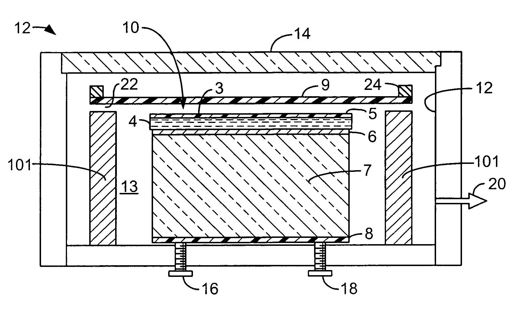
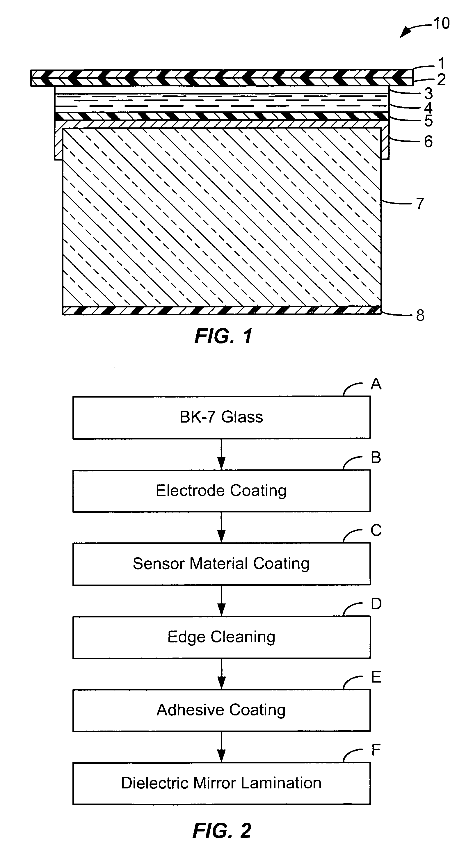
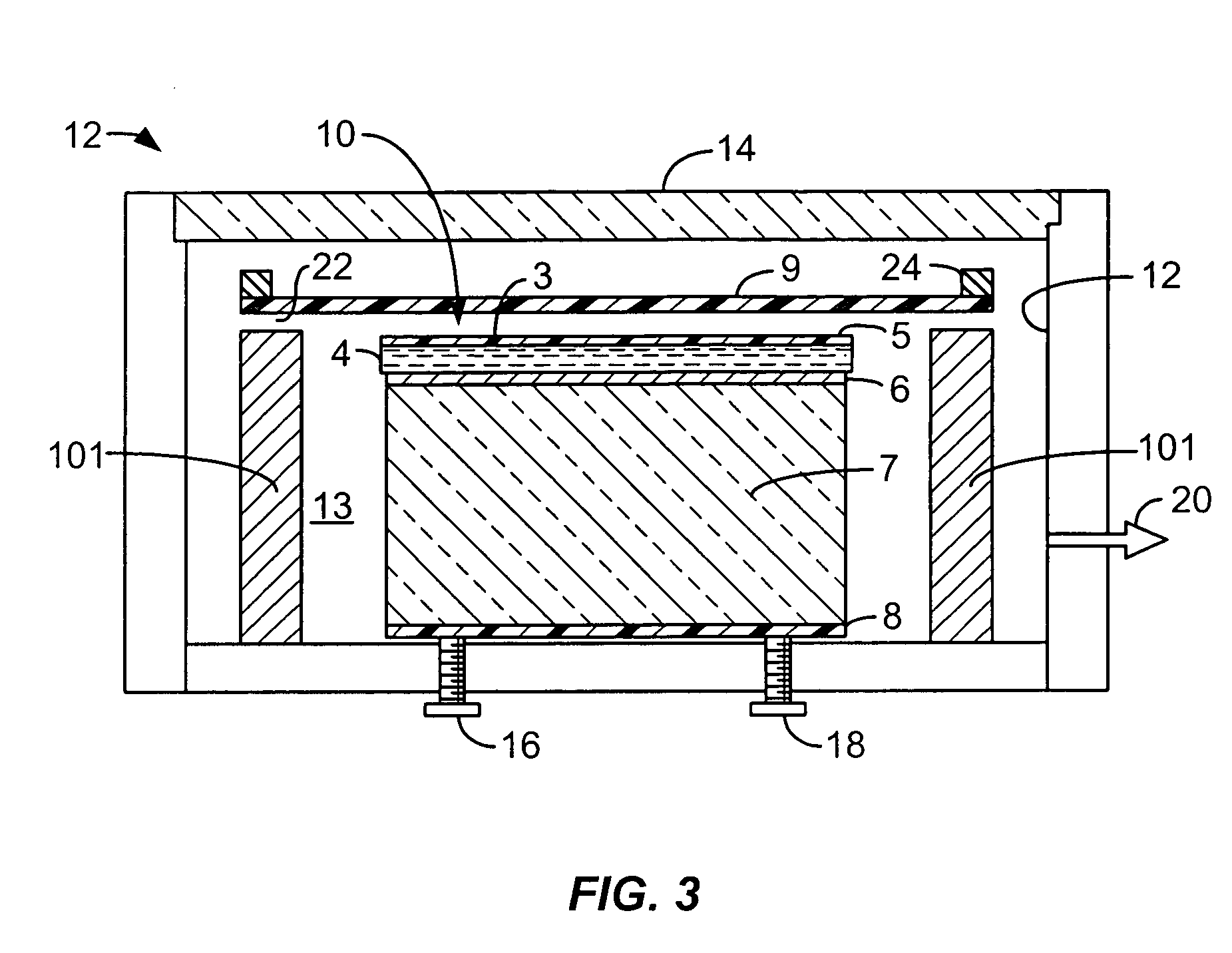
[0017] Referring to FIG. 1, there is shown an electro optic (EO) sensor 10 of an EO modulator fabricated in accordance with the invention. A polyester film layer 1, which is typically a thin Mylar™ film, provides substrate support for a dielectric mirror 2. The substrate / mirror combination is bonded via a thin layer of adhesive 3 to a layer of electro-optic sensor material, specifically a coating of polymer dispersed liquid crystal (PDLC) 4. The PDLC 4 is a directly applied coating on an optional layer of silicon dioxide 5. There is a layer of a transparent electro material, such as indium tin oxide (ITO 6) which in turn is bonded directly to an optical glass substrate 7, which is for example a block of type BK-7 optical glass. The glass substrate or block 7 is optically flat and has an antireflective coating 8 on the optically-smooth surface opposing the PDLC 4 surface.

[0018] Referring to FIG. 2, the process of fabricating the EO sensor 10 according to the invention is illustrated...


PUM

PropertyMeasurementUnit
thickaaaaaaaaaa
vacuumaaaaaaaaaa
angleaaaaaaaaaa

Abstract

In an electro-optic light modulator requiring an electro-optical sensor material such as polymer dispersed liquid crystal, or PDLC is directly coated on an optical glass substrate with a transparent electrode, such as indium tin oxide (ITO) and an optional layer of passivation coating such as silicon dioxide (SiO2) on its surface. A thin layer of polymeric adhesive is coated on top of PDLC layer and then this two-layer coating is laminated with a dielectric mirror on a polyester film (Mylar™) preferably with the assistance of a vacuum.

Description

CROSS-REFERENCES TO RELATED APPLICATIONS [0001] NOT APPLICABLE STATEMENT AS TO RIGHTS TO INVENTIONS MADE UNDER FEDERALLY SPONSORED RESEARCH OR DEVELOPMENT [0002] NOT APPLICABLE REFERENCE TO A “SEQUENCE LISTING,” A TABLE, OR A COMPUTER PROGRAM LISTING APPENDIX SUBMITTED ON A COMPACT DISK [0003] NOT APPLICABLE BACKGROUND OF THE INVENTION [0004] This invention relates to electro-optical sensor material coatings for use in electro-optic applications. More particularly, this invention relates to direct PDLC (polymer dispersed liquid crystal) coating processes on a glass substrate. [0005] Voltage imaging technology may be employed to detect and measure for defects in flat panel thin film transistor (TFT) arrays. According to this measurement technique, the performance of an array is simulated as if it were assembled into a TFT cell and then the characteristics of a TFT array are measured by indirectly measuring actual voltage distribution on the panel, or so-called voltage imaging, using ...

Claims


Application Information

Patent Timeline
Patent Type & Authority Applications(United States)
IPC IPC(8): B32B7/12B32B17/10B32B27/36B32B37/12C03C17/42G02F1/1334G02F1/1362
CPCB32B7/12B32B17/10018B32B17/10174B32B27/36B32B37/003G02F2001/136254B32B2309/06B32B2309/68C03C17/42C03C2217/478G02F1/1334B32B37/12G02F1/136254C03C27/00G02F1/135
Inventor CHEN, XIANHAIBALDWIN, DAVIDNAGY, ALEXANDER
Owner PHOTON DYNAMICS
Why Eureka
Try Eureka