Lanthanide oxide/zirconium oxide atomic layer deposited nanolaminate gate dielectrics

a technology of lanthanide oxide and zirconium oxide, which is applied in the field of lanthanide oxide/zirconium oxide atomic layer deposited nanolaminate gate dielectrics, dielectric layers, etc., can solve the problems of most commonly used gate dielectrics, siosub>2/sub>, and inconvenient use,

Inactive Publication Date: 2005-04-14
MICRON TECH INC
View PDF2 Cites 170 Cited by
  • Summary
  • Abstract
  • Description
  • Claims
  • Application Information

AI Technical Summary

Problems solved by technology

In this thickness range the most commonly used gate dielectrics, SiO2, is not suitable because of leakage current caused by direct tunneling.
There are many known high-k unilaminate dielectric materials with high dielectric constants, such as Ta2O5, TiO2 and SrTiO3, but unfortunately these materials are not thermally stable when formed directly in contact with silicon.
In addition, the interface of such materials need to be coated with a diffusion barrier, which not only adds process complexity, but also defeats the purpose of using the high-k dielectric.
Moreover, materials having too high or too low a dielectric constant may not be an adequate choice for alternate gate applications.
On the other hand, materials with relatively low dielectric constant such as Al2O3 and Y2O3 do not provide sufficient advantage over the SiO2 or Si3N4.
One striking feature of RS-ALD is the saturation of all the reaction and purging steps, which makes the growth self-limiting.
Unfortunately however, although considerable effort was put into use of ALD for growth of silicon and germanium films, difficult precursor chemistry precluded success in this area.

Method used


Image

  • Lanthanide oxide/zirconium oxide atomic layer deposited nanolaminate gate dielectrics
  • Lanthanide oxide/zirconium oxide atomic layer deposited nanolaminate gate dielectrics
  • Lanthanide oxide/zirconium oxide atomic layer deposited nanolaminate gate dielectrics

Examples


Embodiment Construction

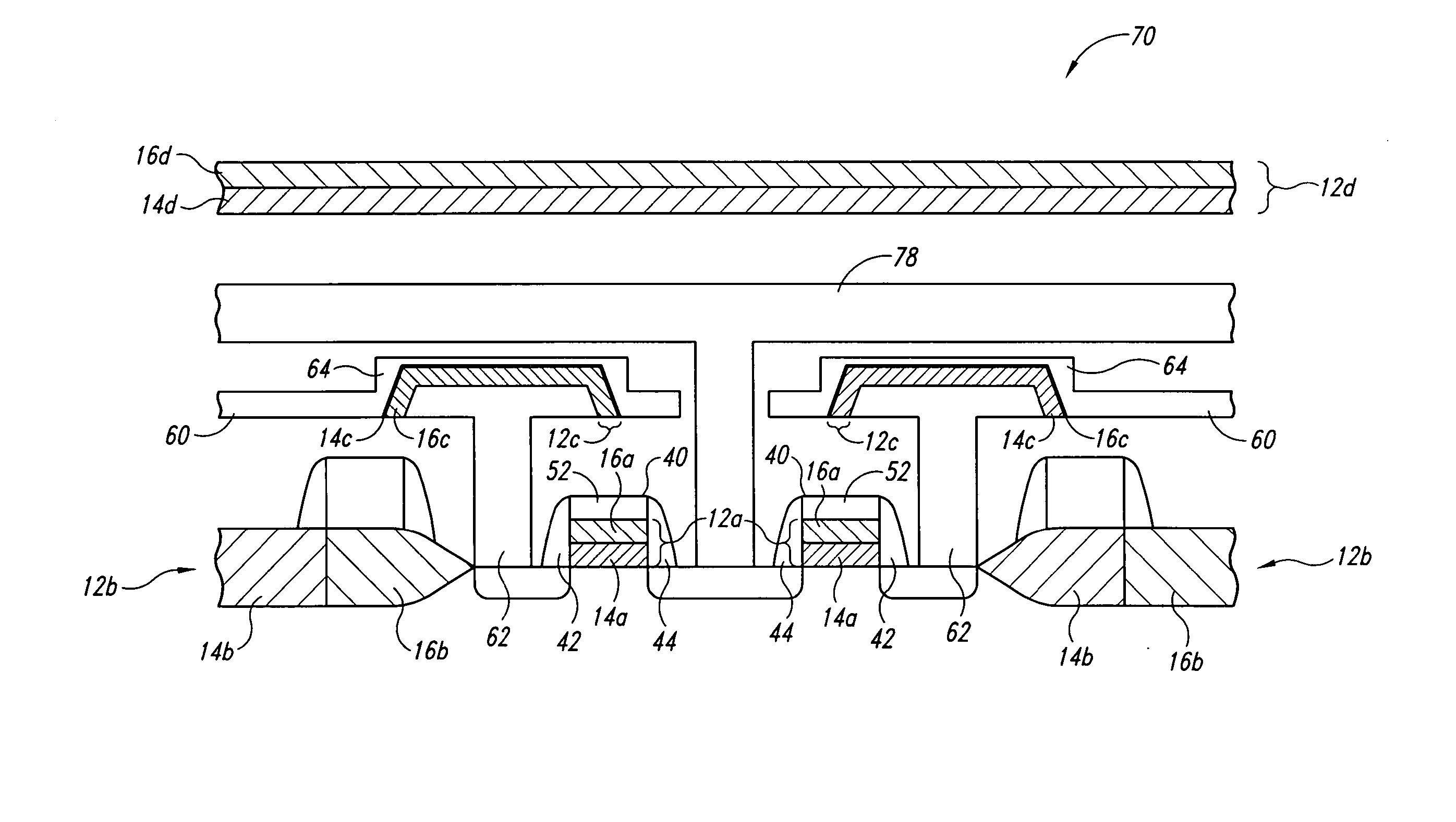
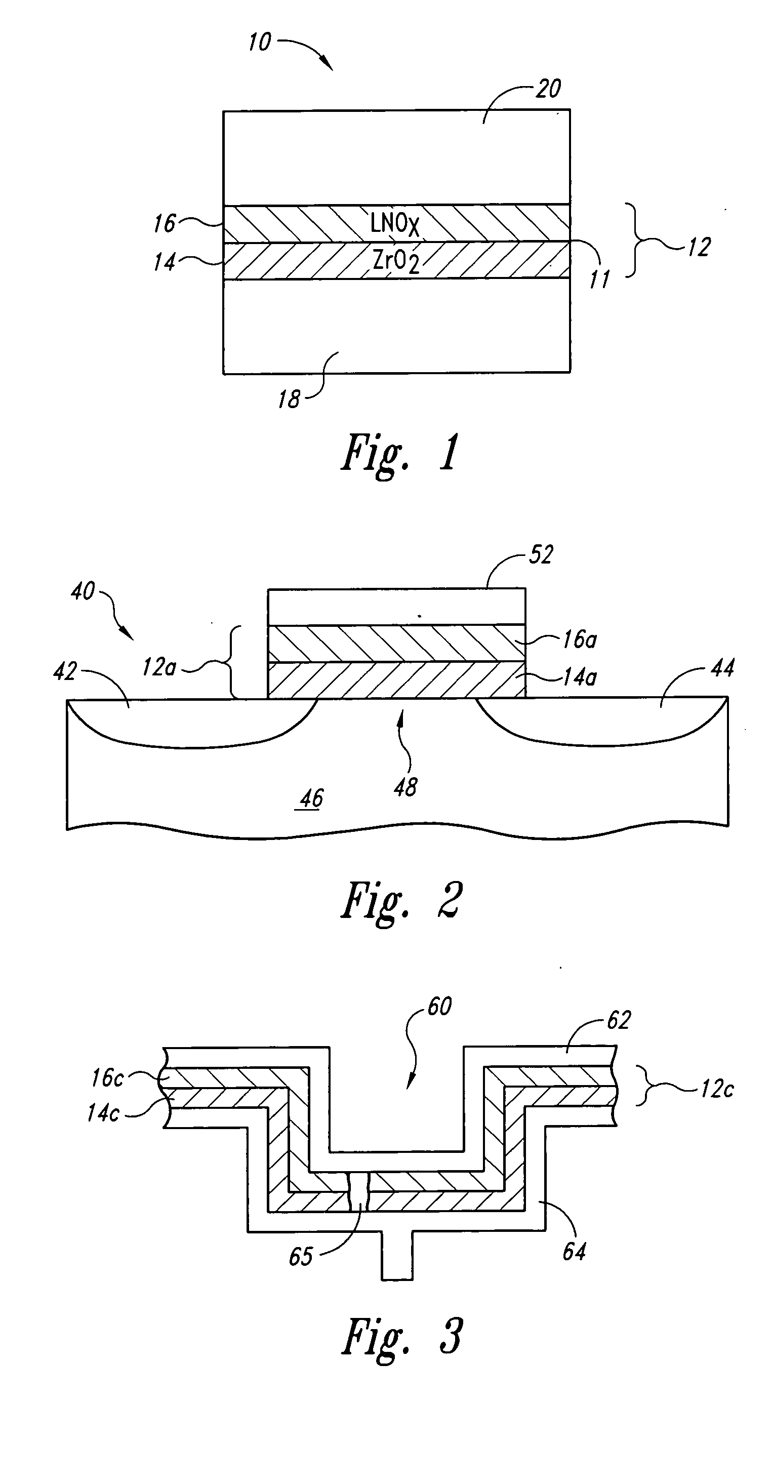
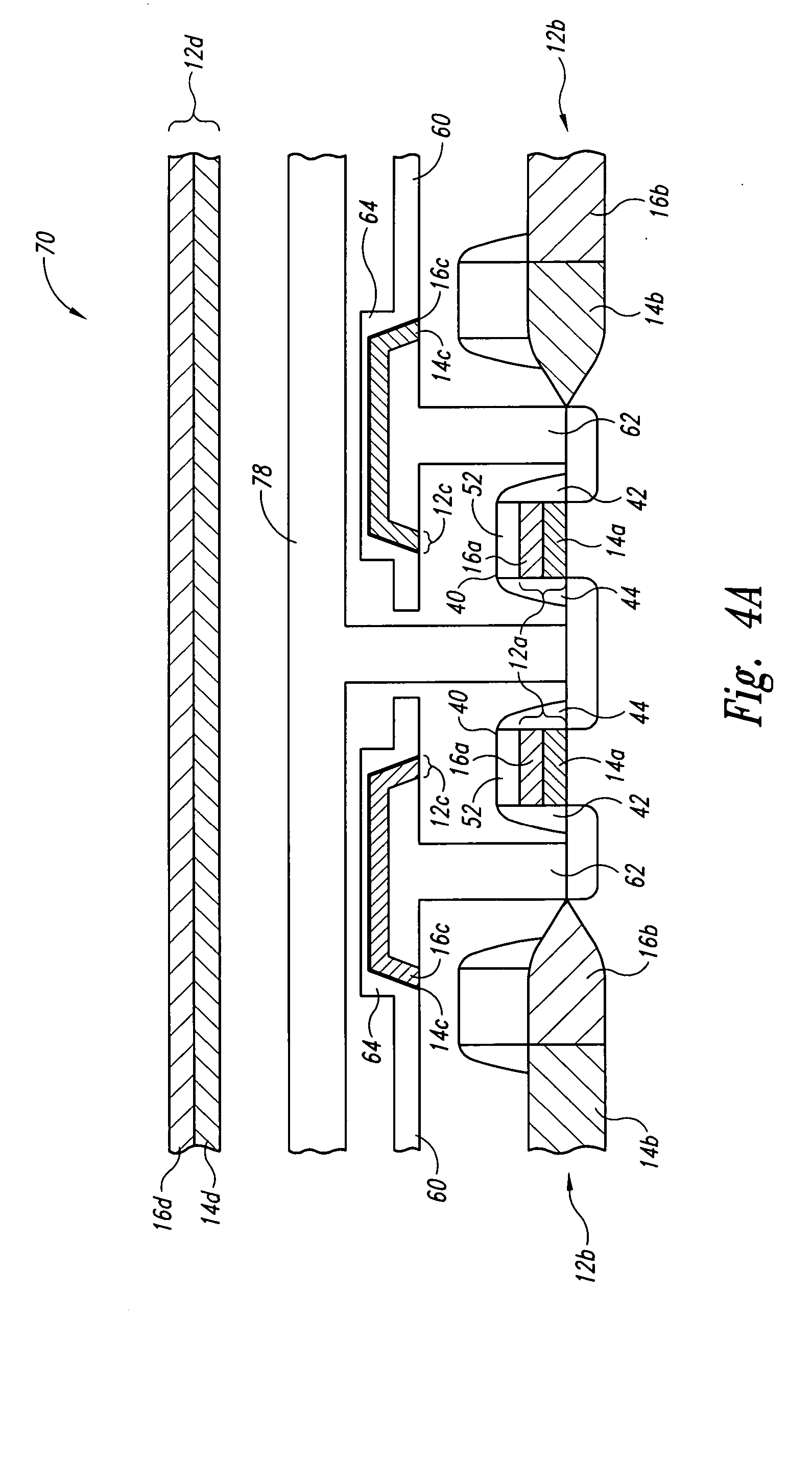
[0019] In setting forth the invention in detail, citation is made to various references that may aid one of ordinary skill in the art in the understanding or practice of various embodiments of the invention. Each such reference is incorporated herein by reference in its entirety, including the references that may be cited in the incorporated references to the extent they may required to practice the invention to its fullest scope. The drawings provided herein are not to scale nor do they necessarily depict actual geometries of the devices of the invention. Rather, the drawings are schematics that illustrate various features of the invention in a manner readily understood by one of ordinary skill in the art, who can make actual devices based on these drawings and the description that follows.

[0020]FIG. 1 depicts a general embodiment of the invention, which includes a semiconductor device 10 that includes a composite laminate dielectric layer 12 made of a ZrO2 first layer 14 laminate...


PUM

PropertyMeasurementUnit
thicknessaaaaaaaaaa
dielectric constantaaaaaaaaaa

Abstract

The invention provides a laminated dielectric layer for semiconductor devices formed by a combination of ZrO2 and a lanthanide oxide on a semiconductor substrate and methods of making the same. In certain methods, the ZrO2 is deposited by multiple cycles of reaction sequence atomic layer deposition (RS-ALD) that includes depositing a ZrI4 precursor onto the surface of the substrate in a first pulse followed by exposure to H2O / H2O2 in a second pulse, thereby forming a thin ZrO2 layer on the surface. After depositing the ZrO2 layer, the lanthanide oxide layer is deposited by electron beam evaporation. The composite laminate zirconium oxide / lanthanide oxide dielectric layer has a relatively high dielectric constant and can be formed in layers of nanometer dimensions. It is useful for a variety of semiconductor applications, particularly for DRAM gate dielectric layers and DRAM capacitors.

Description

TECHNICAL FIELD [0001] The invention relates to the field of semiconductor dielectric layers, and particularly to dielectric layers used in the formation of transistor gates and capacitors in dynamic random access memory devices. BACKGROUND OF THE INVENTION [0002] Dynamic Random Access Memory Devices (DRAMs) have become the standard type of storage device in modern computer systems. Modern DRAMs are high density, highly integrated structures having a variety of configurations, most typically stacked and trench configurations. As ever increasing density is sought, more sophisticated manufacturing processes and materials are required to achieve sub micron sized electrical component layers with reliable conformity to operational specifications. [0003] As density increases, the minimum feature sizes of DRAM components approach 100 nm and smaller. For example, the gate dielectric material thickness of MOS devices may be required to be 20 nm (200 Å) or less in certain designs. In this thi...

Claims


Application Information

Patent Timeline
Patent Type & Authority Applications(United States)
IPC IPC(8): C23C14/08C23C16/40H01L21/00H01L21/28H01L21/31H01L21/314H01L21/469H01L21/8242H01L29/51
CPCC23C14/08C23C16/405H01L21/28194H01L29/517H01L27/1085H01L27/10873H01L29/513H01L21/3142H01L21/02269H01L21/02189H01L21/02192H01L21/0228H01L21/022H10B12/03H10B12/05
Inventor AHN, KIEFORBES, LEONARD
Owner MICRON TECH INC
Why Eureka
Try Eureka