Organic light emitting element and a light emitting device using the same

a light emitting element and light emitting device technology, applied in the direction of discharge tube/lamp details, luminescnet screen, discharge tube/lamp details, etc., can solve the problems of poor color conversion efficiency of blue to red, ineffective back light used for the conventional liquid crystal display device, and deterioration of contrast, etc., to achieve high light emission efficiency, low power consumption, and high efficiency

Active Publication Date: 2005-04-14
SEMICON ENERGY LAB CO LTD
View PDF5 Cites 122 Cited by
  • Summary
  • Abstract
  • Description
  • Claims
  • Application Information

AI Technical Summary

Benefits of technology

[0038] By practicing the present invention, a white organic light-emitting element having high light emission efficiency can be provided. Especially, a high efficient white organic light-emitting element, which has the peak intensity in each wavelength region of re

Problems solved by technology

Further, since the organic light-emitting element is a self-luminous element in which an electroluminescent layer emits light, a back light used for the conventional liquid crystal display device is unnecessary.
However, in case of adopting the CCM method, there has been a problem in red color since color conversion efficiency of from blue to red is poor in principle.
In addition, there has been a problem that the contrast becomes deteriorated since a color conversion material itself is fluorescent so that light is

Method used


Image

  • Organic light emitting element and a light emitting device using the same
  • Organic light emitting element and a light emitting device using the same
  • Organic light emitting element and a light emitting device using the same

Examples


embodiment 1

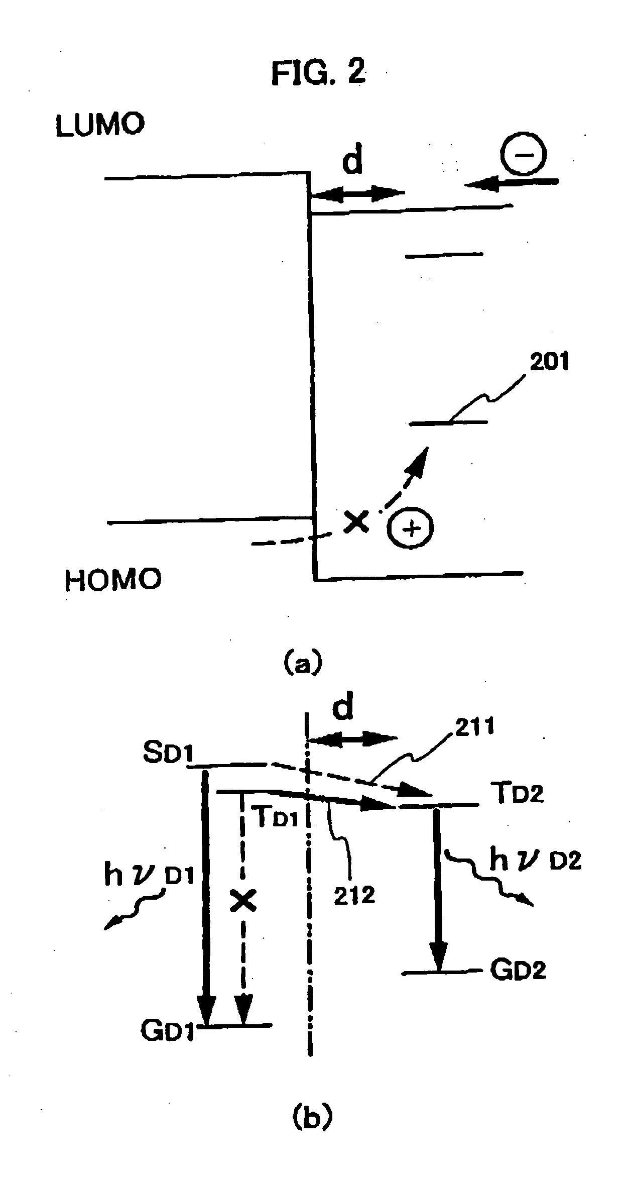
[0052] In what follows, of embodiments of the invention, principles of operation and specific examples of configuration are cited and detailed. In an organic light-emitting element, in order to extract emission, any one of electrodes has only to be transparent. Accordingly, not only an existing element structure in which a transparent electrode is formed on a substrate and light is extracted from a substrate side but also a structure in which light is actually extracted from a side opposite to the substrate and a structure in which light is extracted from both sides of an electrode can be applied.

[0053] Firstly, of an existing white organic light-emitting element that has two emission regions, that is, a first emission region and a second emission region a maximum peak of an emission spectrum of which is located in a longer wavelength side than the first emission region, an example of a basic configuration thereof is shown in FIG. 9.

[0054]FIG. 9 shows a structure of an organic lig...

example 1

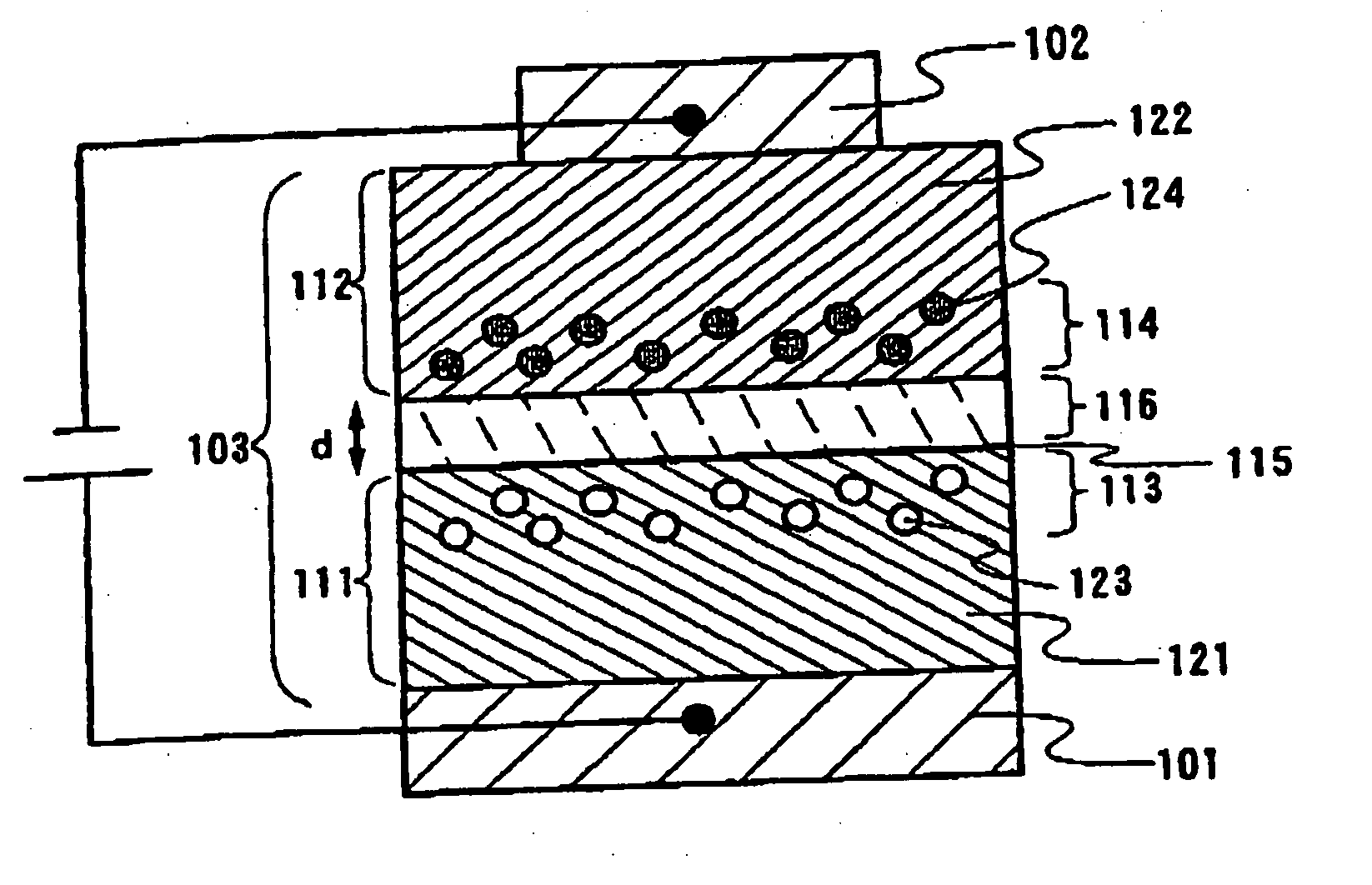
[0090] In the present example, an organic light-emitting element according to the invention and having a gap layer thickness d of 10 nm will be specifically illustrated with reference to FIG. 3. In FIG. 3, reference numerals 301, 302 and 303, respectively, denote an anode, a cathode and an electroluminescent layer.

[0091] Firstly, on a glass substrate on which ITO that is an anode 301 was deposited with a thickness of substantially 100 nm, CuPc that is a hole transport material was deposited with a thickness of 20 nm, and thereby a hole injection layer 310 was formed. Subsequently, α-NPD that is a hole transport material was deposited with a thickness of 30 nm, and thereby a hole transport layer 311 was formed. In the last 10 nm thereof, α-NPD (host material) and perylene (guest material) that is a singlet emission material were co-deposited so as to be substantially 99:1 in the ratio thereof (weight ratio). That is, at a concentration of substantially 1 weight percent, perylene is ...

example 2

[0099] In the present example, an organic light-emitting element according to the invention and having a gap layer thickness d of 20 nm will be specifically illustrated with reference to FIG. 3.

[0100] Firstly, the first emission region 313 is formed similarly to example 1. After the first emission region 313 is formed, BAlq that is a hole block material (and an electron transport material) was deposited with a thickness of 20 nm and thereby a gap layer 316 was formed. BAlq was further deposited with a thickness of 20 nm as an electron transport layer 312. In the first 10 nm thereof, a region to which a phosphorescent material PtOEP was added was co-deposited to form. An addition amount was controlled so that in BAlq PtOEP may be dispersed at a concentration of substantially 7.5 weight percent. This becomes a second emission region 314. Thus, a layer that uses BAlq becomes in sum total 40 nm in combination of the gap layer 316 and the electron transport layer 312.

[0101] In the next...


PUM

PropertyMeasurementUnit
Timeaaaaaaaaaa
Distanceaaaaaaaaaa
Distanceaaaaaaaaaa

Abstract

The present invention provides a white organic light-emitting element high in the emission efficiency. In particular, the invention provides a white organic light-emitting element that has an emission spectrum having peaks in the respective wavelength regions of red color, green color and blue color and is high in the emission efficiency.
Since a spectrum region lowest in the emission efficiency is a red region, by introducing a reddish phosphorescent material, a highly efficient white organic light-emitting element is obtained. At this time, in order to inhibit the reddish phosphorescent material from singularly emitting, as shown in FIG. 1, a distance between a second emission region 114 where a reddish phosphorescent material 124 is a luminescent material and a first emission region 113 that exhibits emission in a shorter wavelength side than the second emission region is separated. In a configuration shown in FIG.1, it is preferable to use an electron transport material in a layer 115 between the first emission region and the second emission region and more preferable to use a hole block material.

Description

TECHNICAL FIELD [0001] The present invention relates to an organic light-emitting element that comprises an anode, a cathode, and a layer containing an organic compound (hereinafter, electroluminescent layer) that generates light by applying electric field through the electrodes; and a light-emitting device that comprises the organic light-emitting element. Specifically, the present invention relates to a light-emitting element that exhibits white emission and a full color light-emitting device comprising the organic light-emitting element. BACKGROUND ART [0002] An organic light-emitting element emits light when electric field is applied thereto. The emission mechanism is a carrier injection type. That is, by applying voltage through a pair of electrodes that interposes an electroluminescent layer therebetween, electrons injected from a cathode and holes injected from an anode are recombined within the electroluminescent layer to form molecules in excited states (hereinafter, excite...

Claims


Application Information

Patent Timeline
IPC IPC(8): H01L51/50H05B33/14
CPCH01L51/5016H01L51/5036H01L51/56H01L51/5028H01L33/502H01L51/5096H10K50/125H10K50/18H10K50/11H10K2101/10H10K50/828H05B33/14H05B33/22H05B33/00H10K50/131H10K50/15H10K50/16H10K50/17H10K50/81H10K50/82H10K50/121H10K50/171H10K59/12H10K59/30H10K71/00H10K85/324H10K85/342H10K85/626H10K85/633
Inventor YAMAZAKI, HIROKOSEO, SATOSHI
Owner SEMICON ENERGY LAB CO LTD
Why Eureka
Try Eureka