Thin film transistor liquid crystal display

a thin film transistor and liquid crystal display technology, applied in non-linear optics, instruments, optics, etc., can solve the problems of reducing the product yield rate, affecting the display quality of the tft lcd panel, and occupying considerable space and consuming more energy, so as to reduce the manufacturing time and cost good light shielding

Active Publication Date: 2005-04-14
INNOLUX CORP
View PDF2 Cites 59 Cited by
  • Summary
  • Abstract
  • Description
  • Claims
  • Application Information

AI Technical Summary

Benefits of technology

[0051] According to the present invention, color filter stacks are formed above the thin film transistors to replace a black matrix, so fabrication time and cost can be reduced.
[0052] The TFT array substrate according to the present invention can use color filter stacks and partially overlapping metal layers at the border of a display area to achieve good light shielding effects.
[0053] The TFT array substrate according to the present invention uses partially overlapping metal layers and color filter blocks at a liquid crystal injection hole of a display area, so good light shielding effects can be achieved, and the size of the liquid crystal injection hole can be increased.

Problems solved by technology

While traditional cathode ray tube (CRT) displays have certain advantages, they take up considerable space and consume more energy.
When the black matrix and the color filters are fabricated on different substrates, misalignment of the back matrix and the color filters may reduce the product yield rate.
Light emitted by circuitry on the substrate 102 can be leaked from the border 110 (FIG. 1) of the display area, adversely affecting the display quality of the TFT LCD panel.
Bursts often occur in the dielectric layer during the repair process, preventing the defective TFT or signal line from being repaired.
Because of imperfections in the microlithography process, such as imperfections in the development of photoresist or etching process, portions of the dielectric layer may remain between the metal layer and the pixel electrode due to incomplete exposure or incomplete etching, resulting in poor electric contact between the metal layer and the pixel electrode.
Such imperfections prevent the storage capacitor from maintaining a specified charge within a specified time to allow the display pixel to show a specified gray level, thus reducing the performance of the display panel.

Method used


Image

  • Thin film transistor liquid crystal display
  • Thin film transistor liquid crystal display
  • Thin film transistor liquid crystal display

Examples


fourth embodiment

THE FOURTH EMBODIMENT

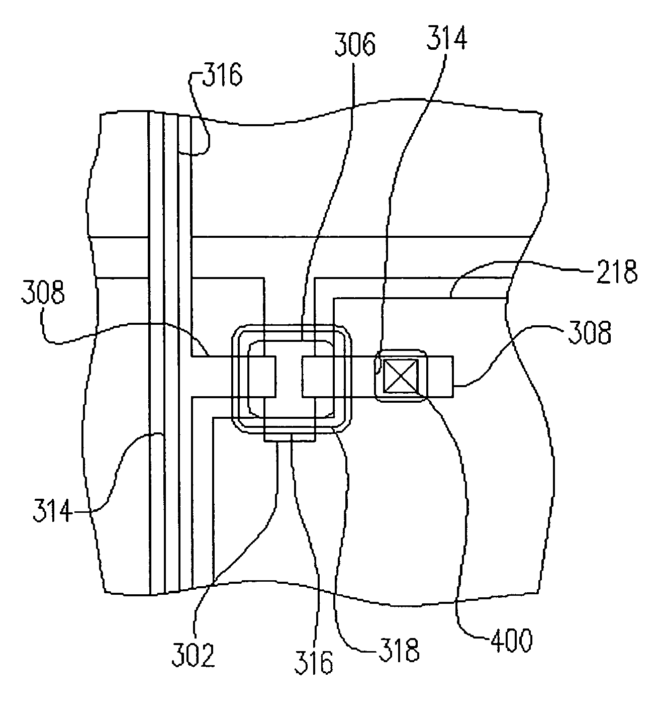
[0096] This embodiment is mainly relates to improvement in the repair structure of the TFT array substrate.

[0097]FIGS. 9A to 9C are cross-sectional process views showing a method of fabricating the TFT array substrate according to a fourth embodiment of the present invention, which can be used with the fabrication process of the first embodiment.

[0098] Referring to FIG. 9A, a first metal layer is formed and patterned on the substrate 202 to form first repair metal layers 902 (there is one first repair metal layer, the plural term “first repair metal layers” refers to multiple portions of the first metal layer) in addition to the structure shown in FIG. 3A. Afterwards, the processing steps are similar to the processing steps of the first embodiment. An insulation layer 304 is formed above the substrate 202. A second metal layer is formed and patterned on the substrate 202 to form second repair metal layers 906 (there is one second repair metal layer, the plural...

fifth embodiment

THE FIFTH EMBODIMENT

[0104]FIGS. 11A to 11C are cross-sectional process views showing a method of fabricating a storage capacitor of the TFT array substrate according to a fifth embodiment of the present invention. The fifth embodiment is similar to the fourth embodiment, wherein the difference between the fifth and fourth embodiments is that, the partially overlapping metal layers of the first metal layer that is formed and patterned above the substrate 202 has first storage capacitor metal layers 1102 (the plural term “first storage capacitor metal layers” refers to multiple portions of the first storage capacitor metal layer), as shown in FIG. 11A, in addition to the structure shown in FIG. 3A. The first storage capacitor metal layer 1102 has first openings 1103, and the first storage capacitor metal layer 1102 can be a part of the scan line or a part of a common line. Afterwards, the processing steps are similar to those of the fourth embodiment. An insulation layer 304 is formed...


PUM

PropertyMeasurementUnit
areaaaaaaaaaaa
coloraaaaaaaaaa
color filteraaaaaaaaaa

Abstract

A thin film transistor (TFT) liquid crystal display (LCD) panel, its array substrate, and its manufacturing method. Color filters are integrated on the TFT array, and color filter stacks are formed on the thin film transistors to replace a black matrix, thereby reducing manufacturing time and costs. The color filter stacks can be placed at the border of the display area of the panel to reduce light leakage. The border of the display area has a liquid crystal injection hole. To allow the size of the liquid crystal injection hole to be increased, and to reduce the light leakage at the hole, color filter blocks and overlapping metal layers can be used at the border of the display area. The color filter stacks and other dielectric layers need to be away from the welding points of repair structures to prevent dielectric layer bursts during a repair process. Storage capacitors can use the feature described above so that the color filters are positioned away from the overlapping portions. Welding is used to improve the electrical contact between the metal layers and the pixel electrode.

Description

BACKGROUND [0001] This invention relates to a liquid crystal display panel, and more particularly to a thin film transistor liquid crystal display having color filters integrated with a thin film transistor array (referred to as color filter on array, abbreviated as COA), its array substrate, and its fabrication method. [0002] With the advancement of technology, video products, particularly digital video or image devices, have become common products in everyday lives. In these digital video or image devices, display devices are important components that allow users to obtain information or to further control the operation of the video or image devices. [0003] The sizes of video or image devices have become thinner and lighter. While traditional cathode ray tube (CRT) displays have certain advantages, they take up considerable space and consume more energy. Using optoelectronics and semiconductor manufacturing technologies, flat panel displays, such as thin film transistor (TFT) liqu...

Claims


Application Information

Patent Timeline
Patent Type & Authority Applications(United States)
IPC IPC(8): G02F1/1343G02F1/1362
CPCG02F1/136209G02F2001/136222G02F1/136259G02F1/136222
Inventor LIN, LIH-NIAN
Owner INNOLUX CORP
Why Eureka
Try Eureka