Method of in-situ monitoring of crystallization state

a crystallization state and insitu monitoring technology, applied in the field of insitu monitoring of crystallization state, can solve the problems of inability to grow crystal grains, inconvenient production control, and uneven growth speed and direction of crystal grain growth, etc., to facilitate production control in a production line, accurate observation, and accurate observation

Inactive Publication Date: 2005-04-14
ADVANCED LCD TECH DEVMENT CENT
View PDF1 Cites 12 Cited by
  • Summary
  • Abstract
  • Description
  • Claims
  • Application Information

AI Technical Summary

Benefits of technology

[0022] According to the present invention, when an annealed thin film is, for example, an amorphous silicon thin film, both the time for melting and crystallizing from when the silicon is melted until it is solidified and crystallized and the speed (information at the position of the monitoring place) of crystal growth (e.g., lateral growth) can be measured. In other words, it is possible to know the position of a boundary face (solid-liquid boundary face) between a solid phase and a liquid phase when the silicon melts and crystallizes and the speed of movement. Since the crystallization state of the silicon thin film can be accurately observed, it is possible to obtain an optimum temperature gradient of the change from melting to solidification of the thin film and an optimum intensity distribution of the energy line (e.g., excimer laser beam) (to obtain an optimum condition), which facilitates production control in a production line.
[0023] Also, according to the present invention, the crystallization state of the silicon thin film can be accurately observed, so that the method and apparatus for in-situ monitoring of the crystallization state can be effectively utilized in developing a high-quality crystallized silicon thin film with few drawbacks as a thin film.
[0024] Also, according to the present invention, a light intensity distribution which includes a temporal change formed in a display screen and related to the position of each place for monitoring can be measured from the temporal change of the intensity distribution of a projected image. Furthermore, by determining a rate of the temporal change of the field in the measuring step in correspondence to the speed of the change from melting to solidification in crystallization of the thin film or promoting the crystallization, it is possible to observe very accurately the change of the film quality from before melting to melting as well as crystallization in the area in the region to be irradiated by the energy line.

Problems solved by technology

The crystallization of the thin film, namely, the speed and direction of growth of the crystal grain as well as the grain diameter are not uniform actually within an area irradiated by an annealing laser beam.
As a result, the crystal grains are not grown as anticipated, and there used to be caused a dispersion in crystallization of the thin film within the area irradiated by the annealing laser beam.
As a result, the crystal grains were not grown inside the thin film as anticipated.
In other words, the melting area of the thin film is not uniform.
A thin film transistor which has undergone laser-anneal processing on the basis of such an erroneous measurement result of crystallization has a feature out of a predetermined range, and a failure, for example, in electrical feature was caused in a liquid crystal display / using this thin film transistor as a switching element or device.

Method used


Image

  • Method of in-situ monitoring of crystallization state
  • Method of in-situ monitoring of crystallization state
  • Method of in-situ monitoring of crystallization state

Examples


Embodiment Construction

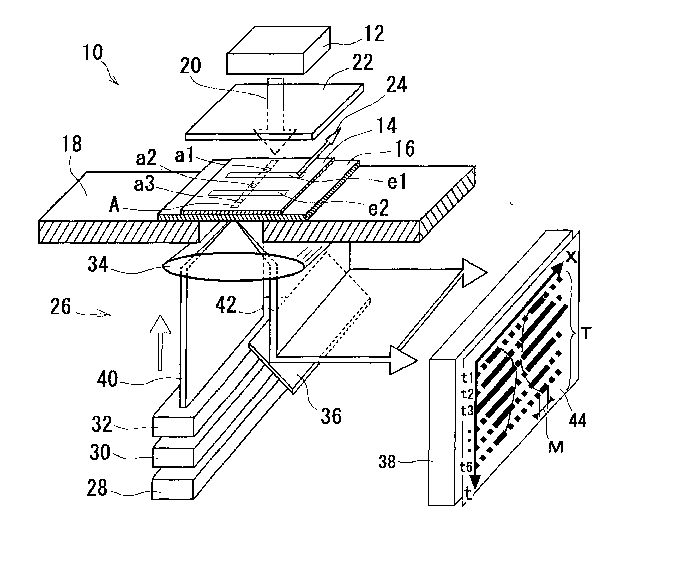
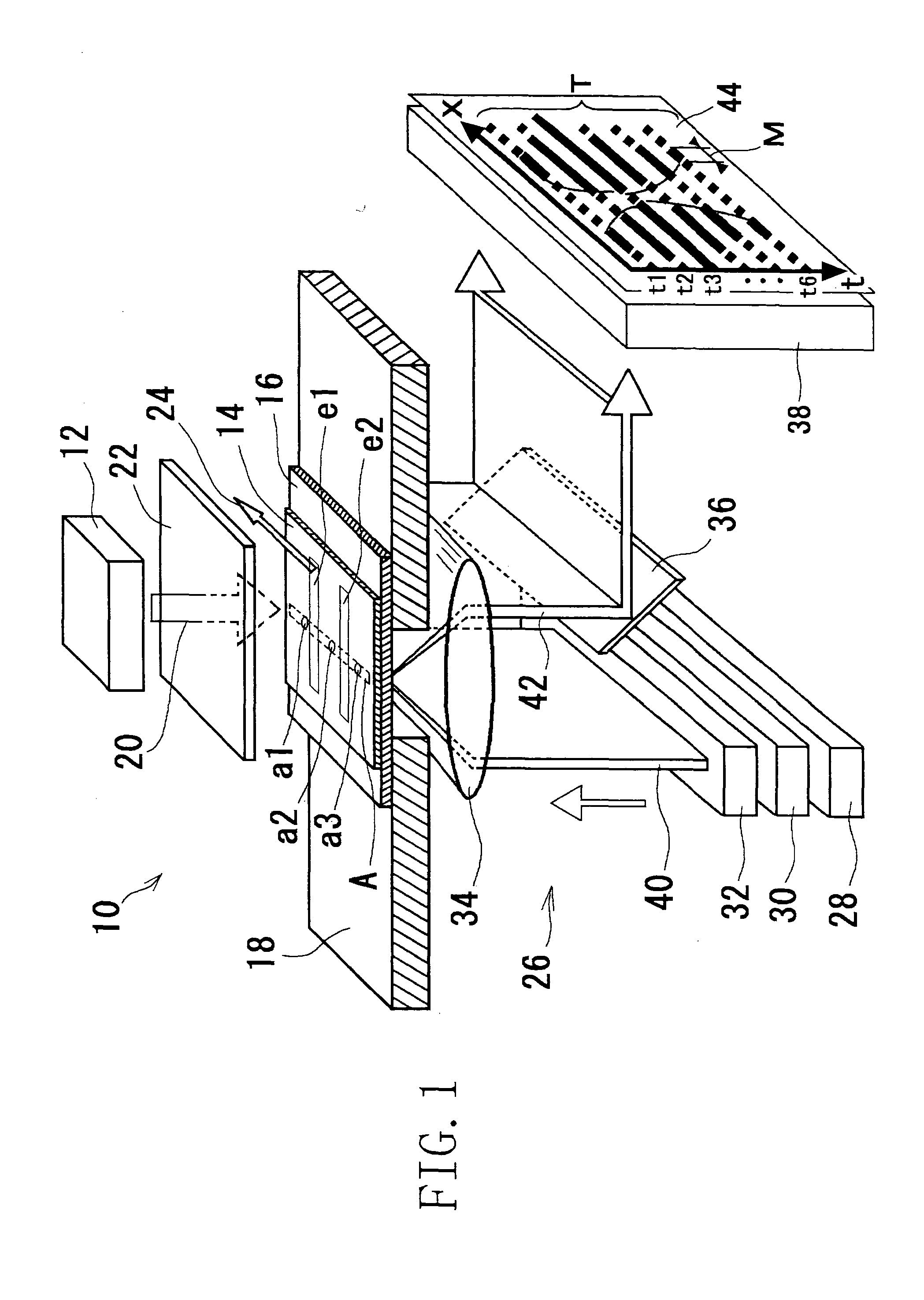
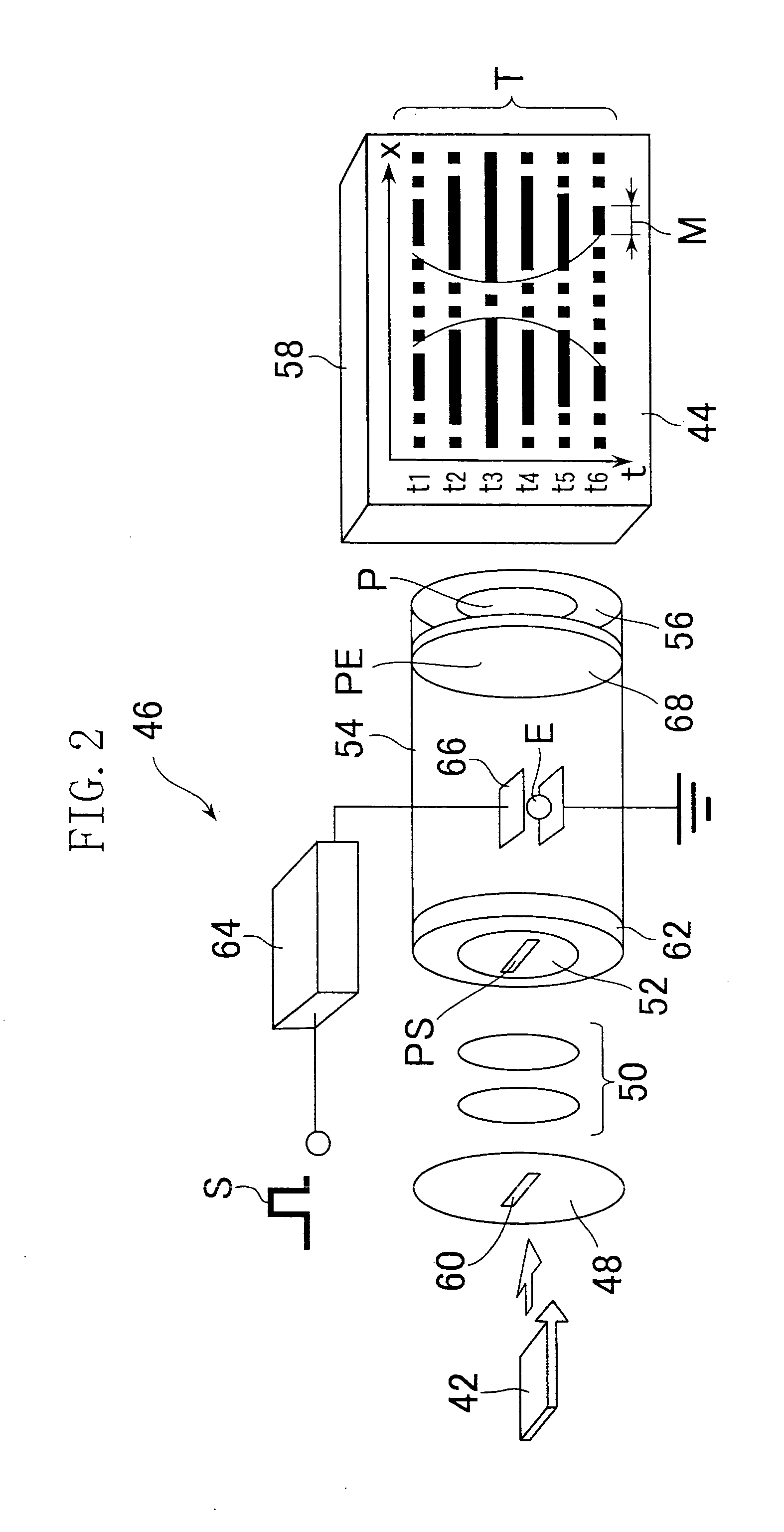
[0043] Referring to FIG. 1, an annealing apparatus 10 using a pulsed laser beam as an energy line is provided with an annealing laser equipment 12, and an XY stage drive mechanism not shown for two-dimensionally moving a sample table 18 which attaches removably a substrate 16 having a thin film 14 to be annealed (hereinafter to be called “annealed thin film 14”). The illustration shows only a part of the sample table 18.

[0044] As a source of an annealing laser beam to be used in the annealing laser equipment 12, it is possible to use, for example, a ruby laser, yttorium aluminium garnet (hereinafter called “YAG”) laser, excimer laser and the like.

[0045] The annealing laser equipment 12 is a pulsed laser light source equipment, which outputs a predetermined energy light necessary for melting an irradiated thin film. The annealing laser equipment 12 usually generates a laser beam having energy of about 1 J per pulse at a pulse time of 20-100 nano seconds (hereinafter called “ns”). I...


PUM

PropertyMeasurementUnit
frequencyaaaaaaaaaa
FWHMaaaaaaaaaa
diameteraaaaaaaaaa

Abstract

A method of in-situ monitoring of a crystallization state is used for laser anneal processing for applying an energy line irradiation for at least one of crystallization of a thin film and promotion of the crystallization. The method of in-situ monitoring of a crystallization state is characterized by irradiating simultaneously at least a plurality of monitoring places in a region having a predetermined area of at least one of the surface and the underside of the thin film by a monitor light for monitoring a crystallization state of the thin film at least during or after of before, during and after the energy line irradiation directly or through a substrate, and measuring a temporal change of the intensity of at least one of a reflected light and a transmitted light, from the surface or the underside of the thin film, of the monitor light as a light intensity distribution related to the positions of the monitoring places.

Description

BACKGROUND OF THE INVENTION [0001] 1. Field of the Invention [0002] The present invention relates to a method and apparatus for in-situ monitoring of a crystallization state to be carried out to monitor the crystallization state of a thin film in a process of anneal processing using an energy line (e.g., laser beam) as well as an annealing method and device using the method of in-situ monitoring of a crystallization state. The method and apparatus for in-situ monitoring of a crystallization state are used, for example, for monitoring the crystallization state when annealing (e.g., laser annealing process) an amorphous semiconductor thin film in a process for producing a thin film transistor for a switching element or device of a liquid crystal display or an organic electroluminescence (hereinafter to be called “EL”) display. [0003] 2. Description of the Prior Art [0004] Conventionally, there has been a method of detecting the intensity of a reflected light from one locally irradiate...

Claims


Application Information

Patent Timeline
Patent Type & Authority Applications(United States)
IPC IPC(8): H01L21/66C30B13/28G01N21/84H01L21/00H01L21/20H01L21/268
CPCC30B13/28G01N21/8422G01N2021/8477H01L21/2026H01L21/67115H01L2924/0002H01L21/67253H01L22/26H01L2924/00H01L21/02686H01L21/02683H01L21/02422H01L21/02678H01L21/02532H01L21/02381H01L22/00
Inventor TAKAMI, YOSHIO
Owner ADVANCED LCD TECH DEVMENT CENT
Why Eureka
Try Eureka