Semiconductor memory device and method of manufacturing the same

a memory device and semiconductor technology, applied in the field ofsr, can solve the problems of increasing the power consumption of an sram, difficult to apply dtmos to a device required, and further difficult to apply dtmos to a device, so as to reduce the increase of power consumption, improve the reliability of operation, and suppress the increase of an area

Inactive Publication Date:
View PDF2 Cites 27 Cited by
  • Summary
  • Abstract
  • Description
  • Claims
  • Application Information

AI Technical Summary

Benefits of technology

An object of the present invention is to improve reliability of operation while suppressing increase of an area for forming an SRAM cell. It is another object of the present invention to reduce increase of power consumption caused by application of a DTMOS.

Problems solved by technology

Therefore, it is difficult to apply the DTMOS to a device required to form a large number of transistors in a small area on a semiconductor substrate.
Therefore, it is further difficult to apply the DTMOS to the SRAM.
Thus, application of the DTMOS to an SRAM cell may increase the power consumption of an SRAM.

Method used


Image

  • Semiconductor memory device and method of manufacturing the same
  • Semiconductor memory device and method of manufacturing the same
  • Semiconductor memory device and method of manufacturing the same

Examples


first preferred embodiment

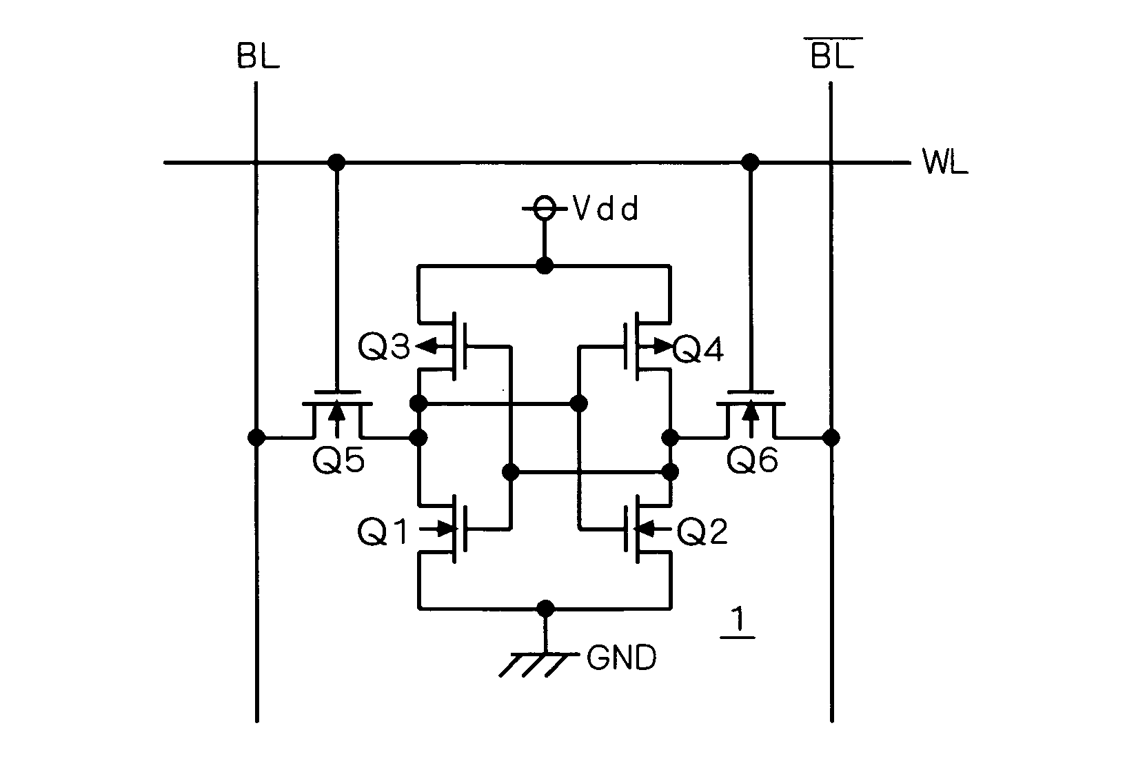
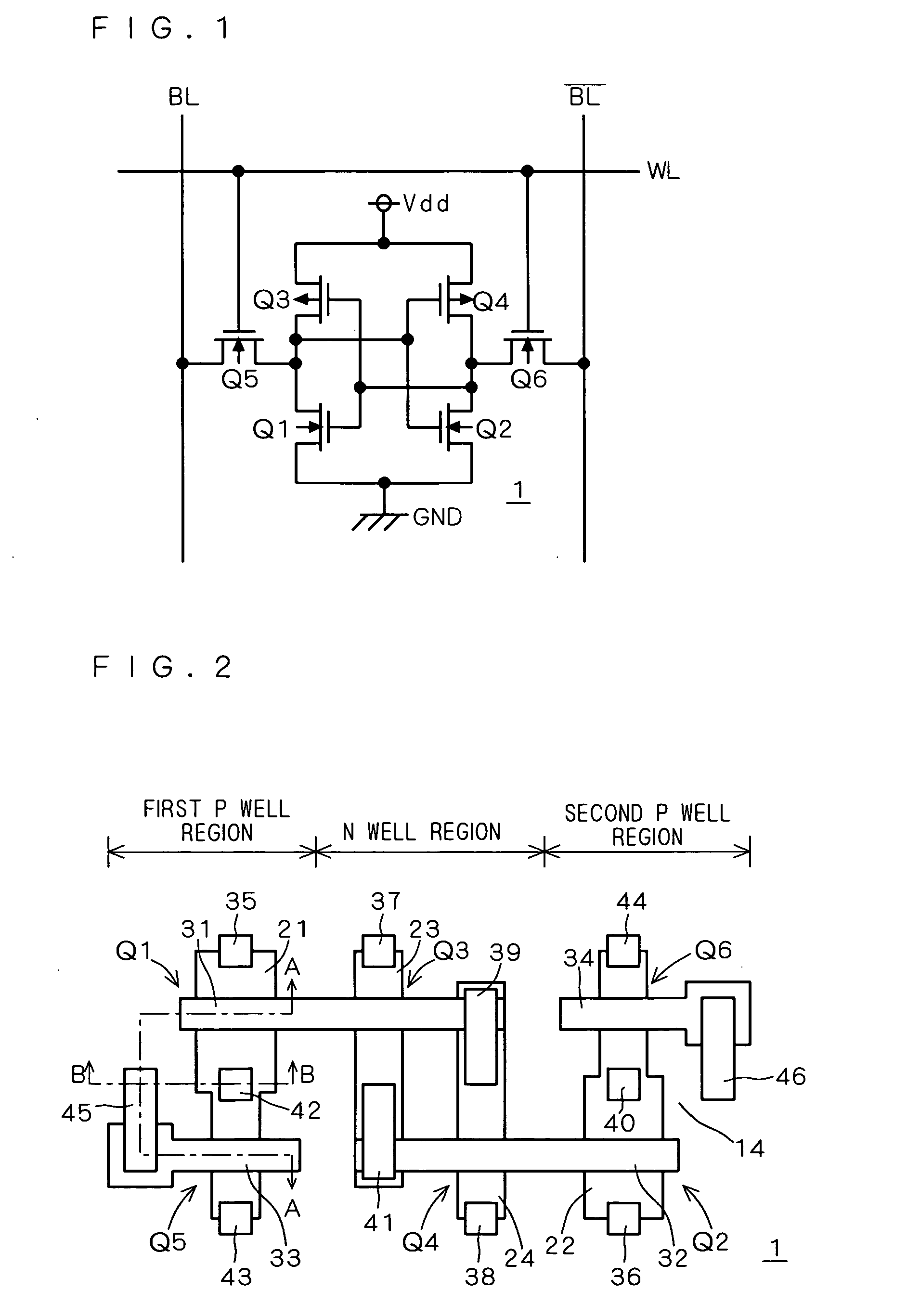
FIG. 1 is a circuit diagram of each memory cell (SRAM cell) 1 of a general SRAM. As shown in FIG. 1, first and second driver transistors Q1 and Q2 which are driving NMOS transistors (driver MOS transistors) and first and second load transistors Q3 and Q4 which are load PMOS transistors (load MOS transistors) constitute a pair of inverters. These inverters are interconnected with each other to constitute a flip-flop circuit. This flip-flop circuit and first and second access transistors Q5 and Q6 which are data transfer NMOS transistors (access MOS transistors) constitute the SRAM cell 1. The gates of the access transistors Q5 and Q6 are connected to a word line WL, while the sources / drains of the access transistors Q5 and Q6 are connected to bit lines BL and / BL respectively.

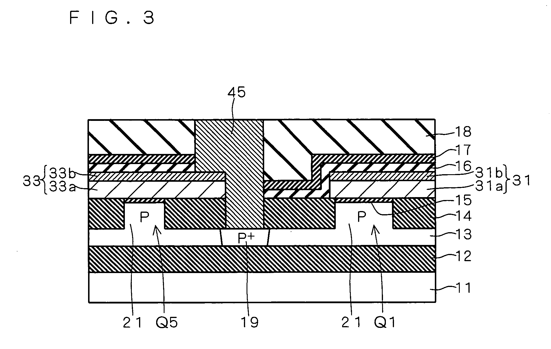
FIG. 2 is a top plan view of each memory cell 1 of an SRAM forming a semiconductor memory device according to a first preferred embodiment of the present invention. As shown in FIG. 2, the SRAM cell 1 comprises...

second preferred embodiment

FIG. 17 is a top plan view of an SRAM cell 1 according to a second preferred embodiment of the present invention. Referring to FIG. 17, elements having functions similar to those of the elements shown in FIG. 2 are denoted by the same reference numerals, to omit redundant description. Also in the second preferred embodiment, a group of a first driver transistor Q1, a first load transistor Q3 and a first access transistor Q5 and a group of a second driver transistor Q2, a second load transistor Q4 and a second access transistor Q6 are similar in structure to each other.

Similarly to the first preferred embodiment, a contact 45 is electrically connected to body regions of the first access transistor Q5 and the first driver transistor Q1 and a contact 46 is electrically connected to body regions of the second driver transistor Q2 and the second access transistor Q6 also in the SRAM cell 1 according to the first preferred embodiment. In other words, FIG. 55 also corresponds to an equiv...

third preferred embodiment

In an SRAM cell 1 according to a third preferred embodiment of the present invention, the DTMOS technique is applied to load transistors Q3 and Q4. FIG. 28 is a top plan view of the SRAM cell 1 according to the third preferred embodiment. Also referring to FIG. 28, elements having functions similar to those of the elements shown in FIG. 2 are denoted by the same reference numerals. The SRAM cell 1 according to the third preferred embodiment has an N-type seventh active region 67 joined to a third active region 23 and an N-type eighth active region 68 joined to a fourth active region 24. The seventh and eighth active regions 67 and 68 are N+ regions having higher impurity concentrations than the remaining portions of the remaining N well regions.

FIGS. 29A and 29B are sectional views of a second load transistor Q4 in the SRAM cell 1 taken along the lines E-E and F-F in FIG. 28 respectively. A first load transistor Q3 is similar in structure to the second load transistor Q4, and henc...


PUM


Abstract

A contact connected to a word line is formed on a gate electrode of an access transistor of an SRAM cell. The contact passes through an element isolation insulating film to reach an SOI layer. A body region of a driver transistor and that of the access transistor are electrically connected with each other through the SOI layer located under the element isolation insulating film. Therefore, the access transistor is in a DTMOS structure having the gate electrode connected with the body region through the contact, which in turn is also electrically connected to the body region of the driver transistor. Thus, operations can be stabilized while suppressing increase of an area for forming the SRAM cell.

Description

BACKGROUND OF THE INVENTION 1. Field of the Invention The present invention relates to a semiconductor memory device, and more particularly, it relates to an SRAM (static random access memory). 2. Description of the Background Art In relation to a MOSFET (metal oxide silicon field-effect transistor) employing an SOI (silicon on insulator) substrate, a DTMOSFET (dynamic threshold voltage MOSFET, hereinafter abbreviated as “DTMOS”) is proposed as means for increasing the operating speed and improving the current driving capability (refer to Japanese Patent Application Laying-Open Gazette No. 2001-77368, pp. 4 to 6, FIG. 3, for example). The SOI substrate has a multilayer structure obtained by stacking a silicon substrate, a buried oxide film (BOX) layer and a silicon layer (SOI layer) in this order. In the DTMOS, a gate electrode having a gate oxide film on the lower surface thereof is selectively formed on the SOI layer. Further, source / drain regions paired through a body region...

Claims


Application Information

Patent Timeline
Patent Type & Authority Applications(United States)
IPC IPC(8): G11C8/02H01L27/11H01L21/8244H01L21/84H01L27/12H01L29/786
CPCH01L21/84H01L27/0207H01L27/11Y10S257/904H01L27/1203Y10S257/903H01L27/1108H10B10/125H10B10/00
Inventor HIRANO, YUUICHIIPPOSHI, TAKASHIMAEGAWA, SHIGETONII, KOJI
Why Eureka
Try Eureka