
Multi-level gate SONOS flash memory device with high voltage oxide and method for the fabrication thereof

a sonos flash memory and high-voltage oxide technology, applied in the direction of sonos flash memory devices, basic electric elements, electrical appliances, etc., can solve the problems of data retention, relatively thick gate oxide layers, and the requirement of high operating speed for surrounding logic functions, so as to avoid additional complexity and expense in the wafer fabrication process

Inactive Publication Date: 2005-04-14
CHARTERED SEMICONDUCTOR MANUFACTURING
View PDF6 Cites 16 Cited by
  • Summary
  • Abstract
  • Description
  • Claims
  • Application Information

AI Technical Summary

Benefits of technology

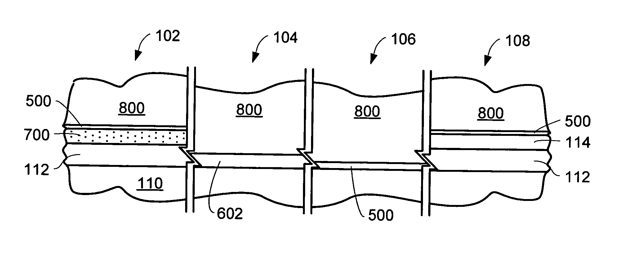
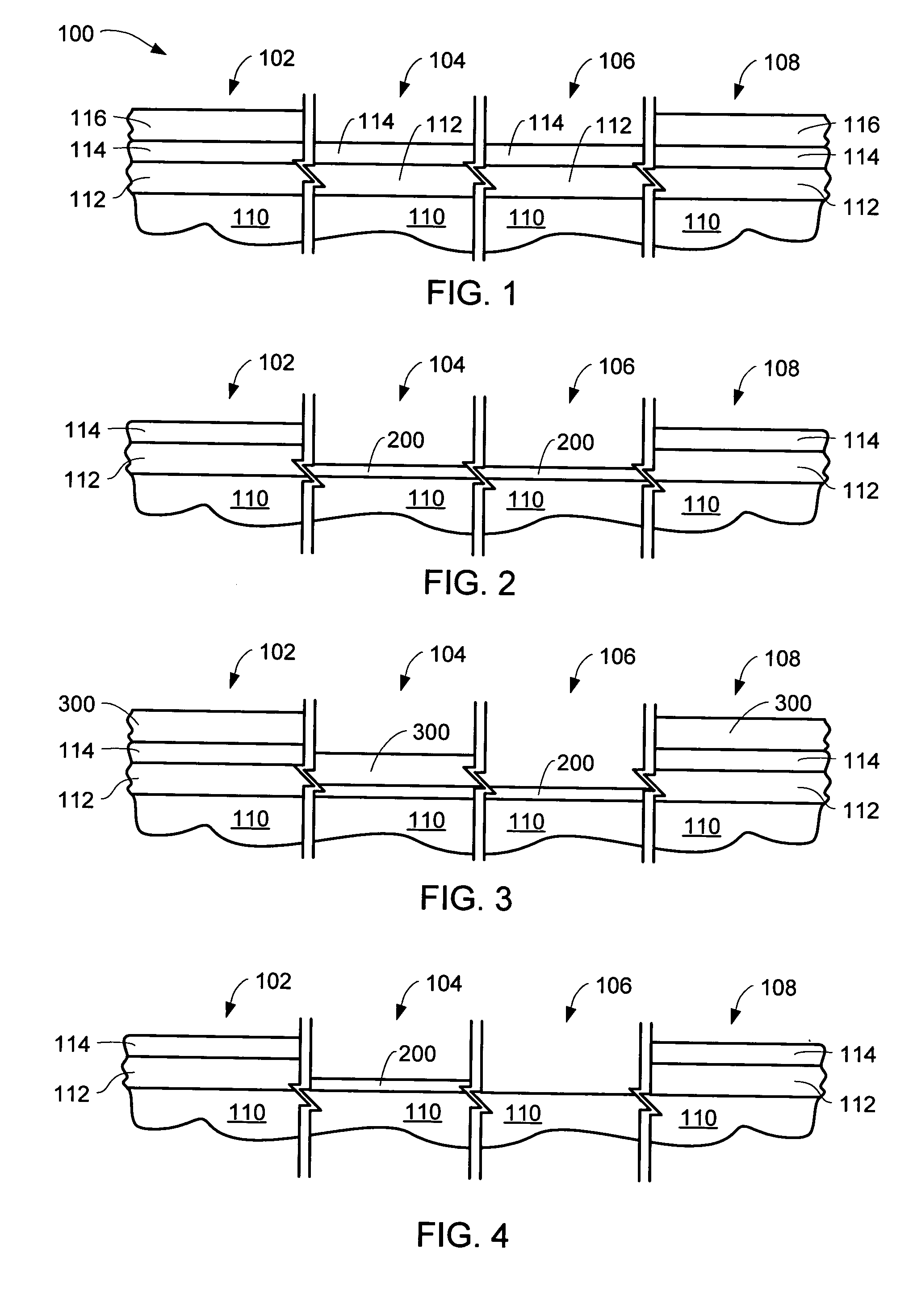
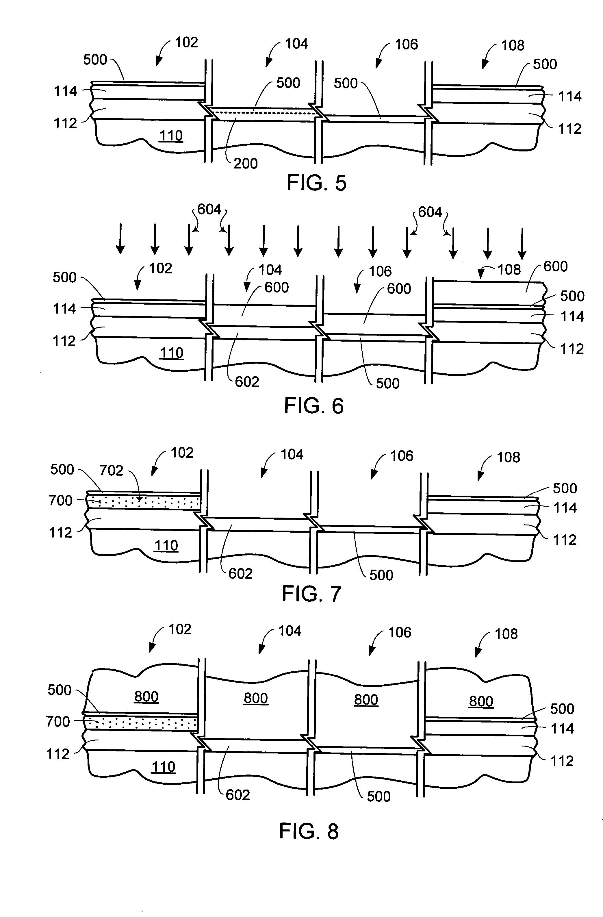
[0015] The present invention provides a method for manufacturing an integrated circuit structure. A semiconductor substrate is provided, and a gate dielectric layer is formed over the semiconductor substrate. The gate dielectric layer is formed in a plurality of thicknesses in a plurality of devices regions over the semiconductor substrate. A second dielectric layer is then formed over at least one of the devices regions. A third dielectric layer is then formed over at least a portion of the second dielectric layer. Ion traps are then selectively implanted in portions of the second dielectric layer. This method provides a means of manufacturing SONOS-type memory devices using existing processing techniques and avoiding additional complexity and expense in wafer fabrication processes.

Problems solved by technology

However, with increasing miniaturization and complexity, these functions are increasingly being located together on the same semiconductor chip or die.
That is, for non-volatile memory devices, the data entry and erase transistors typically require high data retention, which also means relatively thick layers of gate oxide.
But the surrounding periphery logic functions require high operating speed, which means relatively thin layers of gate oxide.
However, other devices that are designed for speed require a thin layer of oxide.
In some instances, it is difficult to form the charge trapping layer over a silicon substrate or gate oxide layer with precision, uniformity, high quality (no defects), and without contamination.
This presents challenges for precisely and uniformly forming ONO sub-layers having predetermined thicknesses.
Thus, important factors toward achieving high performance SONOS cells include the thickness, quality, and cleanliness of the ONO structure, which cannot be sufficiently guaranteed with many known fabrication techniques.
Another disadvantage with SONOS type memory devices is the high temperature process that is needed to make the ONO structures.
This high heat can cause undesirable distortion of prior structures already formed on the semiconductor die.
Solutions to these problems have been long sought but prior developments have not taught or suggested any solutions and, thus, solutions to these problems have long eluded those skilled in the art.

Method used


Image

  • Multi-level gate SONOS flash memory device with high voltage oxide and method for the fabrication thereof
  • Multi-level gate SONOS flash memory device with high voltage oxide and method for the fabrication thereof
  • Multi-level gate SONOS flash memory device with high voltage oxide and method for the fabrication thereof

Examples


Embodiment Construction

[0026] Memory and logic technologies have largely evolved along separate paths. In memory technology, for any particular lithography and power supply voltage level, the gate oxide thickness is limited by thin oxide reliability due to the stress of voltage-boosted functions. In contrast, for logic technology, thinner gate oxide thicknesses are generally the standard due to the need for high performance at lower internal operating voltages. Therefore, efforts to merge the technologies of memory and logic onto a single chip create a dilemma, i.e., the design choice of either (1) compromising the gate oxide thickness for one and / or both types of devices, or (2) assuming the complexities and expenses associated with forming two separate thicknesses (thickness levels) of gate oxides on a single chip.

[0027] Another configuration requiring multi-level gate oxide layers is metal oxide semiconductor (“MOS”) devices, when combined p-channel MOS (“PMOS”) and n-channel MOS (“NMOS”) devices are ...


PUM


Abstract

A method for manufacturing an integrated circuit structure includes providing a semiconductor substrate and forming a gate dielectric layer over the semiconductor substrate. The gate dielectric layer is formed in a plurality of thicknesses in a plurality of devices regions over the semiconductor substrate. A second dielectric layer is formed over at least one of the devices regions. A third dielectric layer is formed over at least a portion of the second dielectric layer. Ion traps are then selectively implanted in portions of the second dielectric layer.

Description

TECHNICAL FIELD [0001] The present invention relates generally to semiconductor integrated circuit devices and methods for the production thereof, and more particularly to devices having non-volatile memories and associated circuits on the same device. BACKGROUND ART [0002] Over the years, developments and improvements in semiconductor performance have been achieved by focusing on a wide range of disciplines. Significant semiconductor improvements have resulted, for example, from device miniaturization, while others have been realized by creating multifunction devices on a single semiconductor chip or die. [0003] Historically, semiconductor devices can be broadly divided into two categories: data processing (logic) devices and data storage (memory) devices. Devices that perform these two different functions have customarily been located on their own separate physical devices. However, with increasing miniaturization and complexity, these functions are increasingly being located toge...

Claims


Application Information

Patent Timeline
IPC IPC(8): H01L21/336H01L21/8246H01L27/105H01L27/115
CPCH01L27/105H01L27/11573H01L27/11568H01L27/115H10B43/30H10B43/40H10B69/00
Inventor ZHENG, ZIA ZHENRAMACHANDRAMURTHY YELEHANKA, PRADEEPLI, WEINING
Owner CHARTERED SEMICONDUCTOR MANUFACTURING
Learn More