

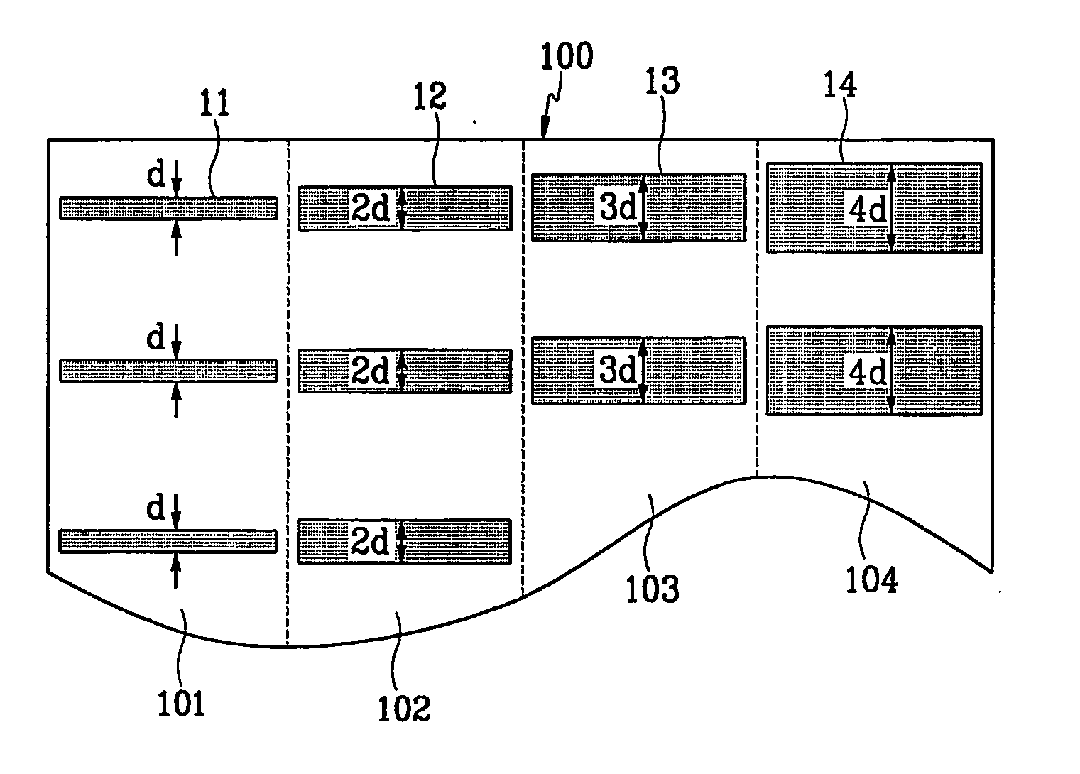
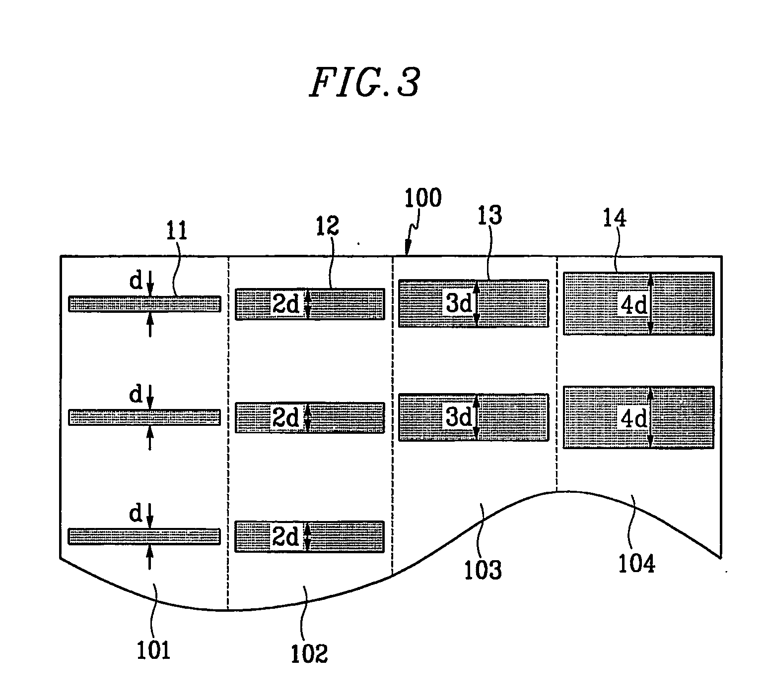
Mask for crystallizing polysilicon and a method for forming thin film transistor using the mask
a polysilicon and mask technology, applied in the field of masks forming polysilicon and thin film transistor fabrication methods, can solve the problems of deteriorating uniformity related to electrical characteristics of neighboring thin film transistors, difficult to employ the techniques for processing liquid crystal panel glass substrates, and limited control of crystalline particle size in a desired manner
- Summary
- Abstract
- Description
- Claims
- Application Information
AI Technical Summary
Benefits of technology
Problems solved by technology
Method used
Image

Examples
Embodiment Construction
[0022] Preferred embodiments of this invention will be explained with reference to the accompanying drawings.
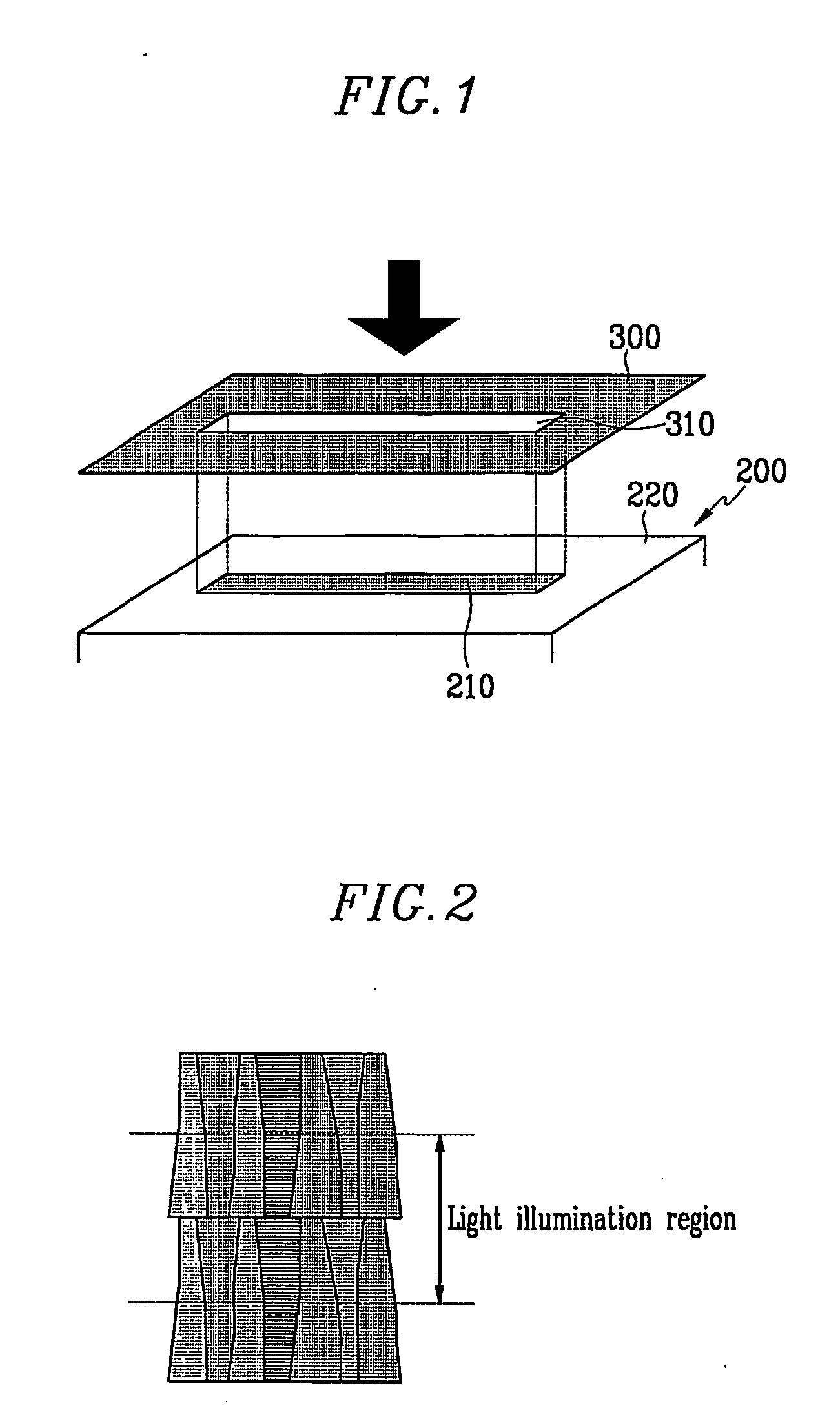
[0023]FIG. 1 schematically illustrates a sequential lateral solidification process where amorphous silicon is crystallized into polysilicon, and FIG. 2 illustrates the micro-structure of the polysilicon during the process.
[0024] As shown in FIG. 1, an amorphous silicon layer 200 is formed on an insulating substrate, and laser beams are illuminated onto the amorphous silicon layer 200 through a mask 300 with a slit-patterned light transmission region 310. The amorphous silicon layer 200 is completely melted in a local manner, and a liquid phase region 210 is formed at the amorphous silicon layer 200 corresponding to the light transmission region 310 of the mask 300. At this time, the grains of the polysilicon are grown from the interface between the laser-illuminated liquid phase region 210 and the non-illuminated solid phase region 220 perpendicular thereto. The grain growt...
PUM
| Property | Measurement | Unit |
|---|---|---|
| temperature | aaaaa | aaaaa |
| transmission | aaaaa | aaaaa |
| width | aaaaa | aaaaa |
Abstract
Description
Claims
Application Information