

Method for forming damascene structure utilizing planarizing material coupled with compressive diffusion barrier material
a damascene and diffusion barrier technology, applied in the manufacture of basic electric elements, semiconductor/solid-state devices, electric devices, etc., can solve the problems of poisoning of the line imaging layer, poisoning problems that are much worse, and methods fraught with problems
- Summary
- Abstract
- Description
- Claims
- Application Information
AI Technical Summary
Benefits of technology
Problems solved by technology
Method used
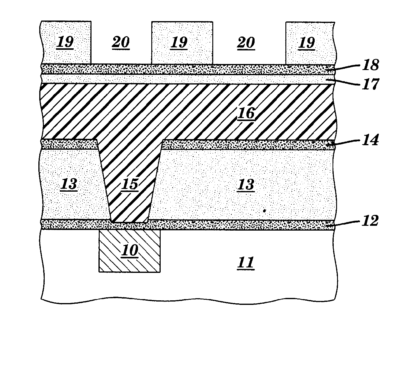
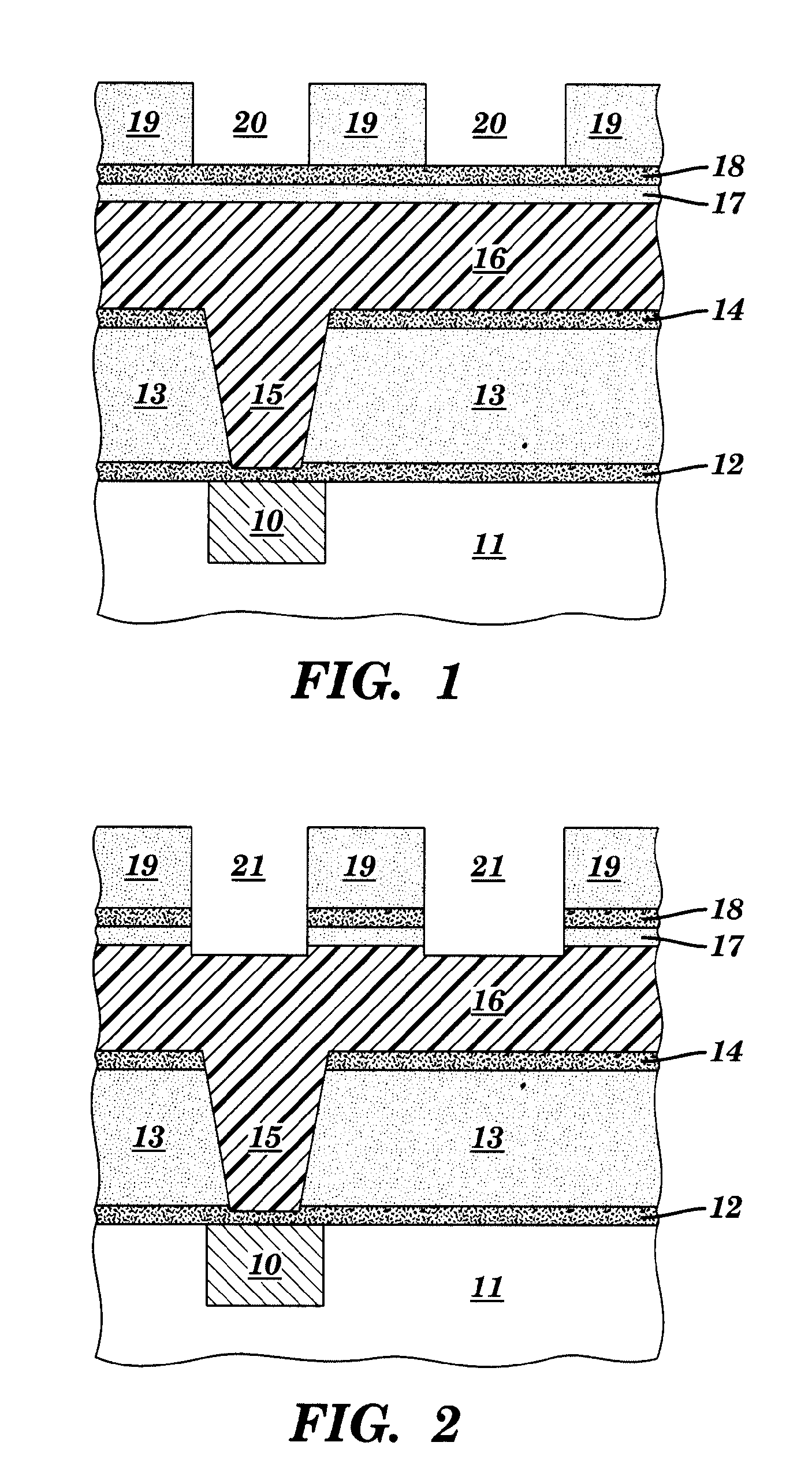
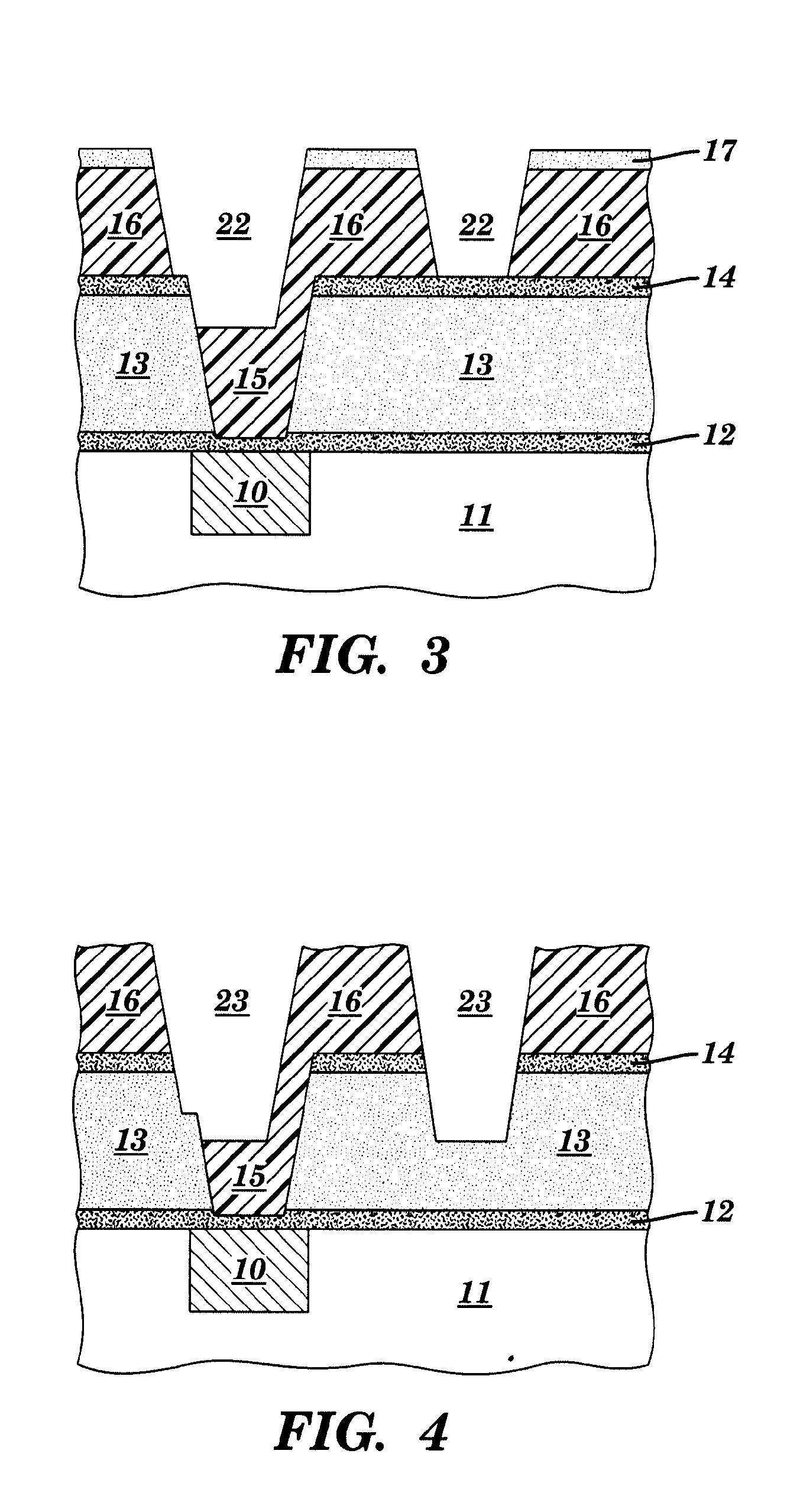
Image

Examples
example i
[0033] The method herein described was successfully utilized in the production of a 90 nm ground rule integrated circuit chips, using the preferred PHS-based system described above as the planarizing layer 16 and LTO as the barrier layer 17. The cap layer 12 above underlying Cu conductors 10 was SiCNH, and no post-treatments or covering layers were used so as to prevent amine formation from this layer. Some chips were fabricated with via resist strip etch chemistries that included N2 and H2, with no cleaning step after this strip. This would tend to form amines after subsequent 225° C. bake of the planarizing layer. The absence of resist poisoning was verified through optical and SEM inspection and through electrical test data. It is known that certain structures on the chip are particularly sensitive to resist poisoning, such as isolated vias and the corners of via chain array test structures. All test structures were shown to be completely free of any resist poisoning effects.
[00...
PUM
| Property | Measurement | Unit |
|---|---|---|
| compressive stress | aaaaa | aaaaa |
| dielectric constant | aaaaa | aaaaa |
| temperature | aaaaa | aaaaa |
Abstract
Description
Claims
Application Information