Selective oxygen-free etching process for barrier materials

a technology of barrier materials and etching processes, which is applied in the direction of basic electric elements, semiconductor/solid-state device manufacturing, electrical equipment, etc., can solve the problems of low selectivity ratio between sin layer and silicon oxide containing dielectric layer, generating undesirable polymers, and damaging copper interconnects, etc., to achieve high selectivity

Active Publication Date: 2005-04-14
LAM RES CORP
View PDF10 Cites 9 Cited by
  • Summary
  • Abstract
  • Description
  • Claims
  • Application Information

AI Technical Summary

Benefits of technology

A method of etching a barrier layer in an integrated circuit (IC) wherein the barrier layer is composed of silicon nitride or silicon carbine. The method comprises receiving an etched IC structure having an etched trench and / or via with an exposed barrier layer. The method then proceeds to apply an etchant gas mixture comprising nitrous oxide (N2O) and a fluoromethane (CH3F) gas. Additionally, the etchant gas mixture may also include an inert diluent gas such as Argon (Ar). The etchant gas mixture provides a relatively high selectivity between the barrier layer to an adjacent silicon containing dielectric layer. The selectivity ratio between SiN to the adjacent silicon containing dielectric material is approximately 1.7 or more.

Problems solved by technology

However, the use of O2 and / or O2 containing gas mixtures has resulted in damaging the copper interconnects.
Thus, the selectivity ratio between a SiN layer to a silicon oxide containing dielectric layer is too low.
Furthermore O2 free gases, such as CH3F, N2, and H2, generate undesirable polymers that are deposited on the IC structure.
Therefore, each of the gas combinations, i.e, O2 containing gas mixtures and O2 free gases, has an associated limitation when etching a barrier layer.

Method used


Image

  • Selective oxygen-free etching process for barrier materials
  • Selective oxygen-free etching process for barrier materials
  • Selective oxygen-free etching process for barrier materials

Examples


Embodiment Construction

In the following detailed description, reference is made to the accompanying drawings, which form a part hereof, and which show illustrative embodiments. These embodiments are described in sufficient detail to enable those skilled in the art to practice the invention, and it is to be understood that other embodiments may be utilized and that structural, logical and process changes may be made without departing from the spirit and scope of the claims. The following detailed description is, therefore, not to be taken in a limited sense. The leading digit(s) of the reference numbers in the Figures corresponds to the figure number, with the exception of identical components that appear in multiple figures and are identified by the same reference numbers.

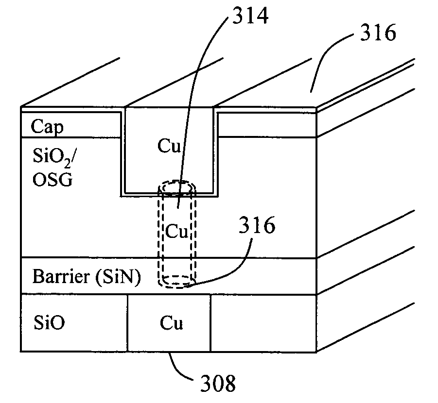
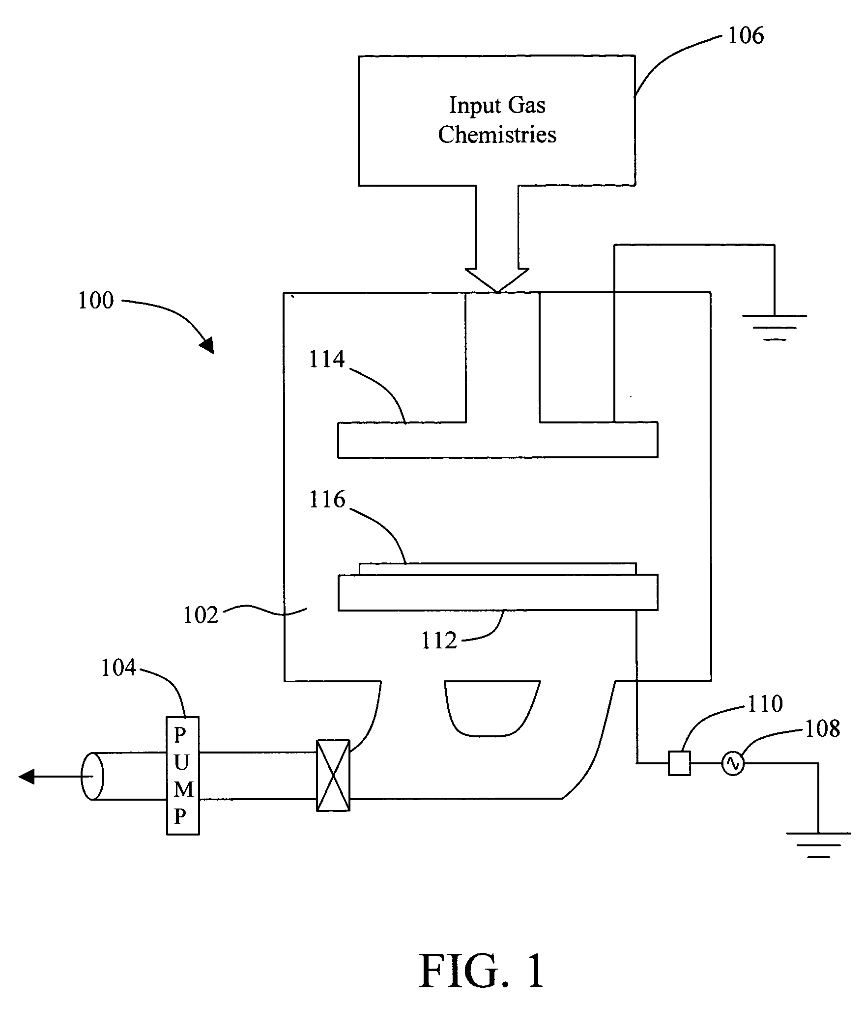
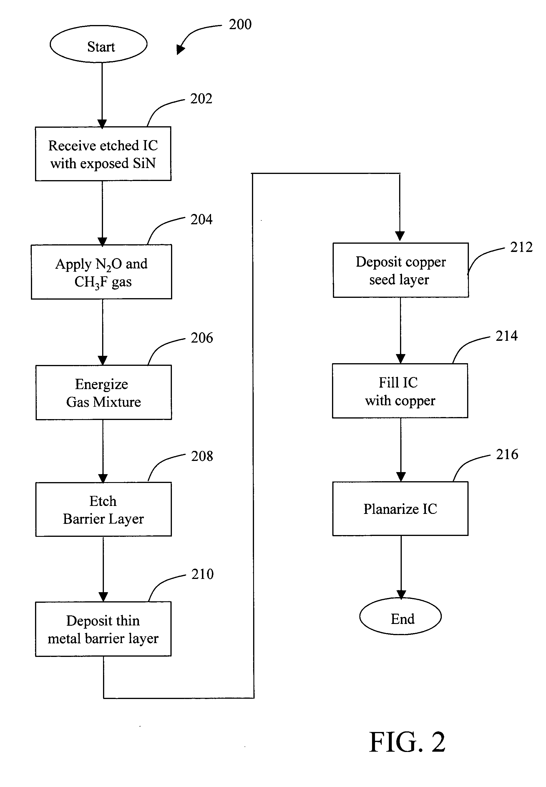
Referring to FIG. 1 there is shown an illustrative system capable of etching a silicon nitride or silicon carbide barrier layer from an IC structure. The illustrative system is also configured to perform hard mask etching, dielectric ...


PUM

PropertyMeasurementUnit
dielectricaaaaaaaaaa
conductiveaaaaaaaaaa
vacuum pressureaaaaaaaaaa

Abstract

A method of etching a barrier layer in an integrated circuit (IC) wherein said barrier layer is composed of silicon nitride or silicon carbide. The method comprises receiving an etched IC structure having an exposed barrier layer. The method then proceeds to apply an etchant gas mixture comprising a nitrous oxide (N2O) gas and a fluoromethane (CH3F) gas. The etchant gas mixture provides a relatively high selectivity between the barrier layer to an adjacent dielectric layer.

Description

BACKGROUND 1. Field of Invention The present invention relates to the etching of a barrier layer. More particularly, the invention relates to the etching of an integrated circuit (IC) structure having a barrier material such as silicon nitride (SiN) and silicon carbide (SiC). 2. Description of Related Art Semiconductor devices are typically formed on a semiconductor substrate and often include multiple levels of patterned and interconnected layers. For example, many semiconductor devices have multiple layers of conductive lines (e.g., interconnects). Conductive lines or other conducting structures, such as gate electrodes, are typically separated by dielectric material (i.e., insulating material) and may be coupled together, as needed, by vias through the dielectric material. During the semiconductor integrated circuit (IC) fabrication process, devices such as component transistors are formed on a semiconductor wafer substrate. Various materials are then deposited on different ...

Claims


Application Information

Patent Timeline
Patent Type & Authority Applications(United States)
IPC IPC(8): H01L21/311H01L21/768
CPCH01L21/76807H01L21/31116
Inventor ZHU, HELENANNAPRAGADA, RAO
Owner LAM RES CORP
Why Eureka
Try Eureka