
Bipolar transistor with a very narrow emitter feature

a bipolar transistor and emitter technology, applied in the field of semiconductor transistors, can solve the problems of increasing the self-heating of the device, increasing the avalanche of electric field, and the collector change of the bipolar transistor has some potentially negative side effects, so as to achieve high-performance device operation, low emitter resistance, and high voltage

Active Publication Date: 2005-04-21
IBM CORP
View PDF4 Cites 10 Cited by
  • Summary
  • Abstract
  • Description
  • Claims
  • Application Information

AI Technical Summary

Benefits of technology

This patent describes a method and structure for creating an emitter with a small size and controllable dimension. The metal contact can be close to the device, reducing emitter resistance. A donut emitter can be formed without an emitter junction in the center of the device, allowing it to sustain higher voltages. The method also addresses issues of high-performance NPN transistors by providing a narrowed window with sidewall spacers. The invention provides a double-polysilicon, self-aligned bipolar transistor with a collector region, intrinsic base, and doped emitter. A narrowing structure is formed with an extrinsic emitter and an emitter below the extrinsic emitter. The technical effects of this invention include small emitter size, controllable dimension, low emitter resistance, and high performance device operation.

Problems solved by technology

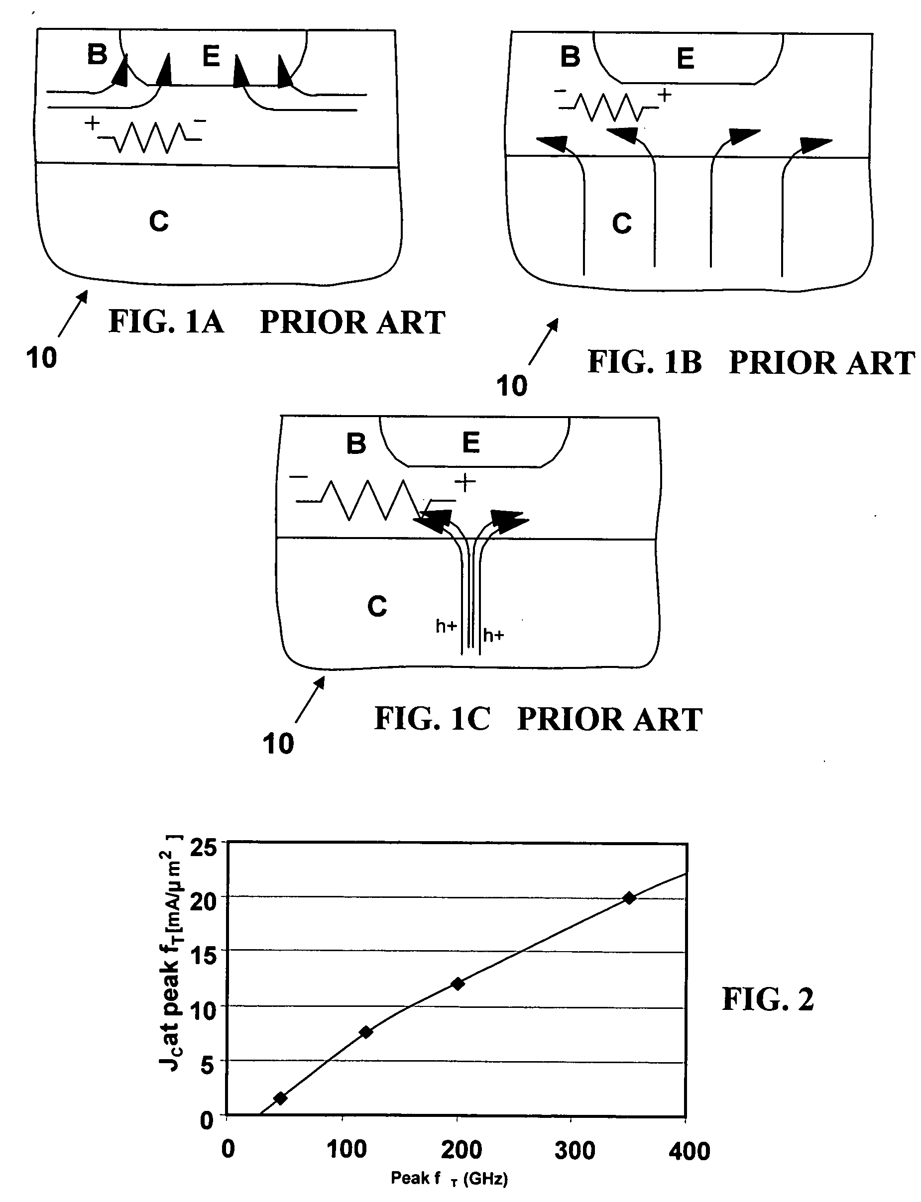
Besides the positive effect of enhancing the switching speed of the device, there are problems in that the changes in the collector of the bipolar transistor have some potentially negative side-effects.
One such problem is the increase of avalanche multiplication from the increased electric field in the collector-base space-charge region.
A second problem is the increase of self-heating of the device.
In particular, as avalanche current increases with device scaling, side-effects, such as pinch-in phenomena, become predominant that limit the maximum attainable voltage in a device.
In pinch-in, the device current is focused into the center of the device, where very high power densities can cause problems in device operation.
However, the problem is that methods or structures, which enhance the voltage capability have not been described.
Yet very narrow dimensions are increasingly difficult to attain. FIG. 2 is a graph showing an empirical trend in the prior art of current density versus device design peak fT.
Yet such techniques are costly and involve constraints such as pattern density, minimum dimensions, and mask data preparation complexities.
Such a resultant dimension may not be made so small that the variation in size of the original opening together with the variation in size of the sidewall spacer may subtract substantially from the expected size, thus rendering the device not useful.
Thus there is an issue with process control and with minimum dimensions achievable with the structure described by Tsai et al.
Furthermore, the large width to height aspect ratio would likely result in a significant emitter resistance, which is detrimental to device performance.
Yet the approach provided by Darwish et al. does not provide for an emitter contact over the emitter region, which is needed to maintain a low emitter resistance for high performance bipolar transistor operation.

Method used


Image

  • Bipolar transistor with a very narrow emitter feature
  • Bipolar transistor with a very narrow emitter feature
  • Bipolar transistor with a very narrow emitter feature

Examples


Embodiment Construction

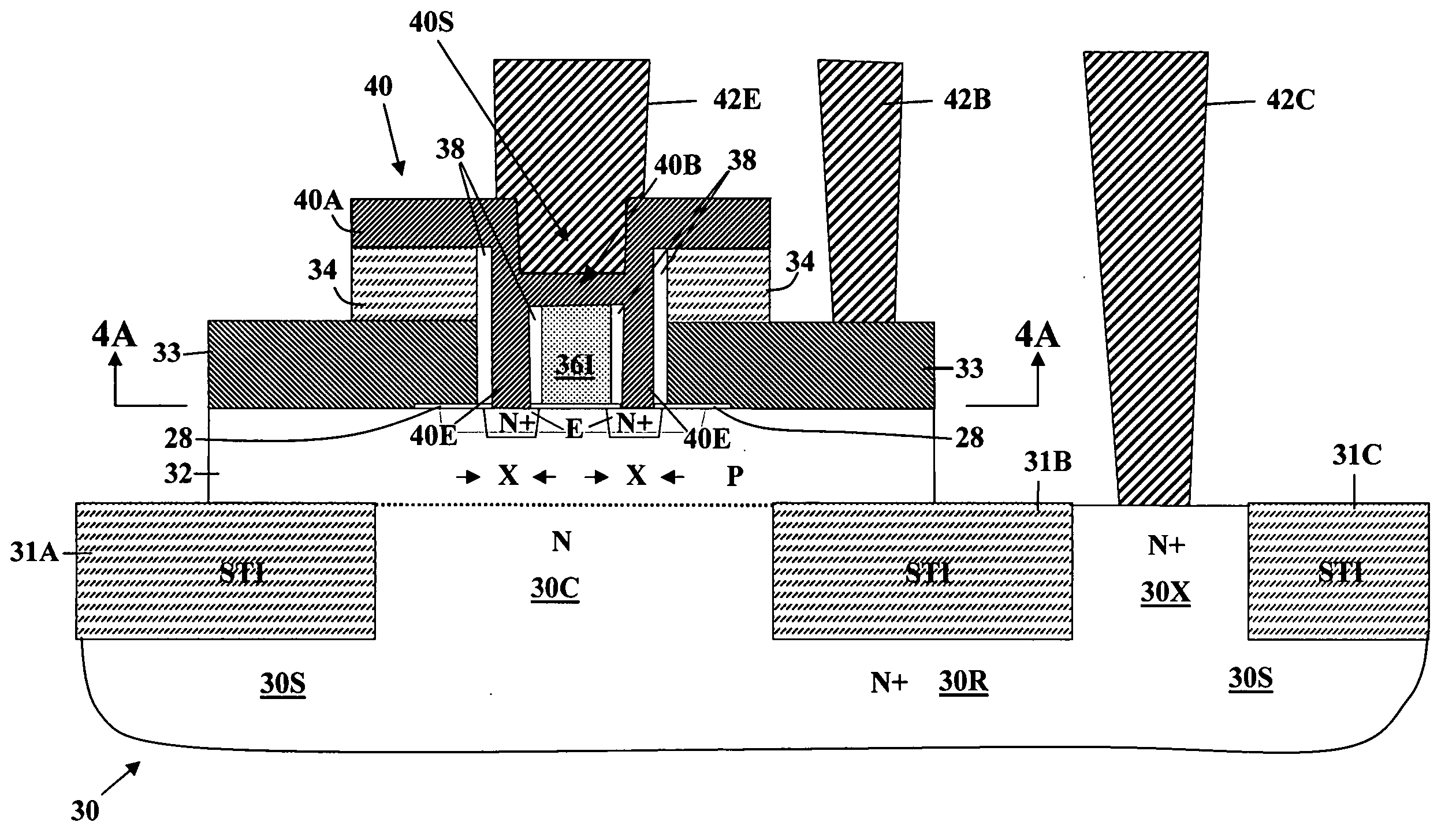
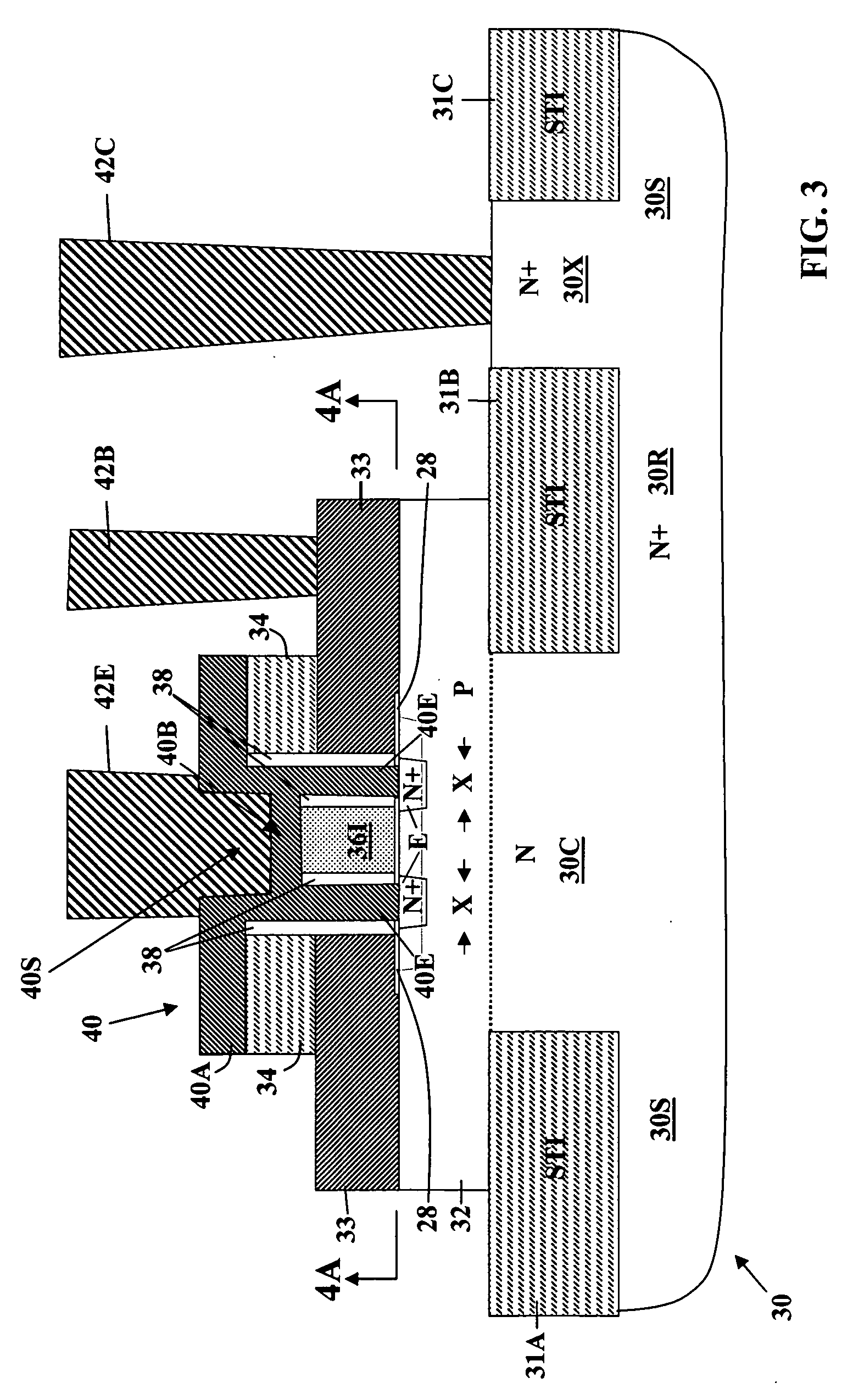
[0029]FIG. 3 shows a bipolar transistor 30 comprising a silicon semiconductor substrate 30S, which is doped with N type dopant, in which a collector region 30C is formed and on which an intrinsic base 32 is formed with dual intrinsic emitter regions E that are juxtaposed thereof. The dual intrinsic emitter regions E are connected to dual extrinsic emitter connectors 40E on either side of a dielectric island 36I and a portion of an etch stop region 28. A plurality of Shallow Trench Isolation (STI) regions 31A, 31B and 31C are formed spaced apart in the surface of the substrate 30S. The collector region 30C is formed between STI regions 31A and 31B in the substrate 30S. The intrinsic base 32 (base layer B) of the bipolar transistor 30 is formed on top of the left portion of the substrate 30S bridging across the collector region 30C and most of the two STI regions 31A and 31B leaving margins thereof not covered by the intrinsic base 32.

[0030] The dual extrinsic emitter regions E are f...


PUM


Abstract

A double-polysilicon, self-aligned bipolar transistor has a collector region formed in a doped semiconductor substrate, an intrinsic counterdoped base formed on the surface of the substrate and a doped intrinsic emitter formed in the surface of the intrinsic base. An etch stop insulator layer overlies the intrinsic base layer above the collector. A base contact layer of a conductive material overlies the etch stop dielectric layer and the intrinsic base layer. A dielectric layer overlies the base contact layer. A wide window extends through the insulator layer and the base contact layer down to the insulator layer. An island or a peninsula is formed in the wide window leaving at least one narrowed window within the wide window, with sidewall spacers in either the wide window or the narrowed window. The narrowed windows are filled with doped polysilicon forming an extrinsic emitter with the intrinsic emitter formed below the extrinsic emitter in the surface of the intrinsic base.

Description

BACKGROUND OF INVENTION [0001] This invention relates to semiconductor transistors and more particularly to a method of manufacture of bipolar transistors with enhanced emitter structures. [0002] In the manufacture of bipolar transistors the trend in the semiconductor industry is to increase the switching speed performance of such transistors. To achieve enhanced switching speed performance, the layers through which the electrons traverse in the bipolar transistors must continually be decreased. Principally, these dimensions are the neutral base dimension and the collector-base space-charge dimension. Scaling the device also involves increasing the collector dopant concentration, which has the aforementioned effect of reducing the collector-base, space-charge dimension. In addition, scaling the device increases the current density at which the device reaches its peak operating speed. [0003] Besides the positive effect of enhancing the switching speed of the device, there are problem...

Claims


Application Information

Patent Timeline
Patent Type & Authority Applications(United States)
IPC IPC(8): H01L21/331H01L29/08H01L29/732
CPCH01L29/0804H01L29/732H01L29/66287
Inventor FREEMAN, GREGORY G.KHATER, MARWAN H.PAGETTE, FRANCOISSTRICKER, ANDREAS D.
Owner IBM CORP
Learn More