Semiconductor test board having laser patterned conductors

a technology of laser patterned conductors and test boards, which is applied in the direction of semiconductor/solid-state device testing/measurement, semiconductor/solid-state device details, instruments, etc., can solve the problems of component non-functionality, defective components on the substrate, and defects in the address circuitry of components,

Inactive Publication Date: 2005-04-21
MICRON TECH INC
View PDF36 Cites 5 Cited by
  • Summary
  • Abstract
  • Description
  • Claims
  • Application Information

AI Technical Summary

Benefits of technology

[0009] In accordance with the present invention, a method for fabricating and testing semiconductor components is provided. A

Problems solved by technology

One shortcoming of wafer level fabrication processes is that some of the components on the substrate can be defective.
For example, defects can occur in the integrated circuits contained on the components, in the address circuitry for the components, or in the configuration of the arrays of semiconductor devices on the components.
Some defects can make a component non-functional, while other defects merely affect the electrical characteristics of the component.
The defective components can decrease the yield of the substrate and affect the quality of the sin

Method used


Image

  • Semiconductor test board having laser patterned conductors
  • Semiconductor test board having laser patterned conductors
  • Semiconductor test board having laser patterned conductors

Examples


Embodiment Construction

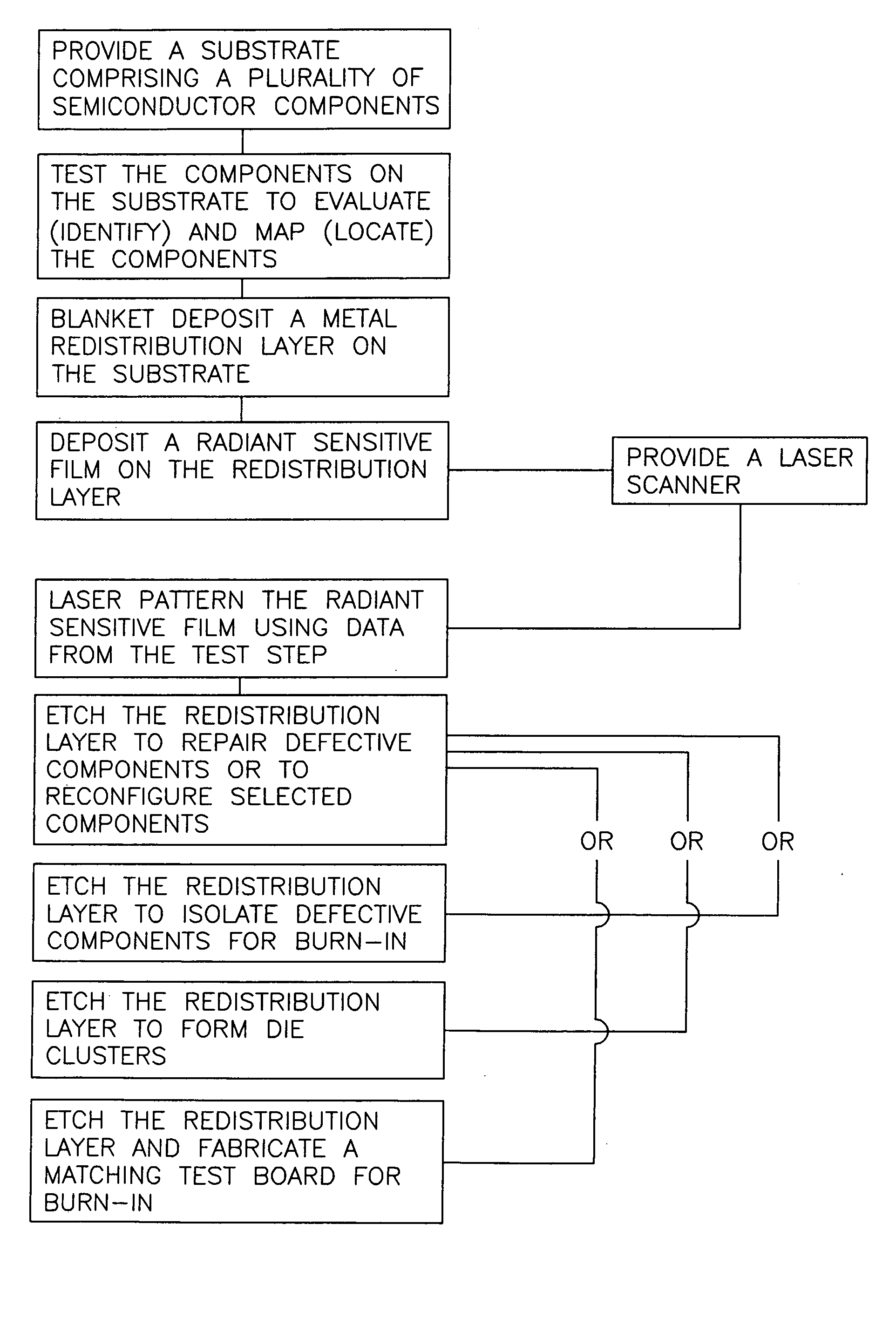
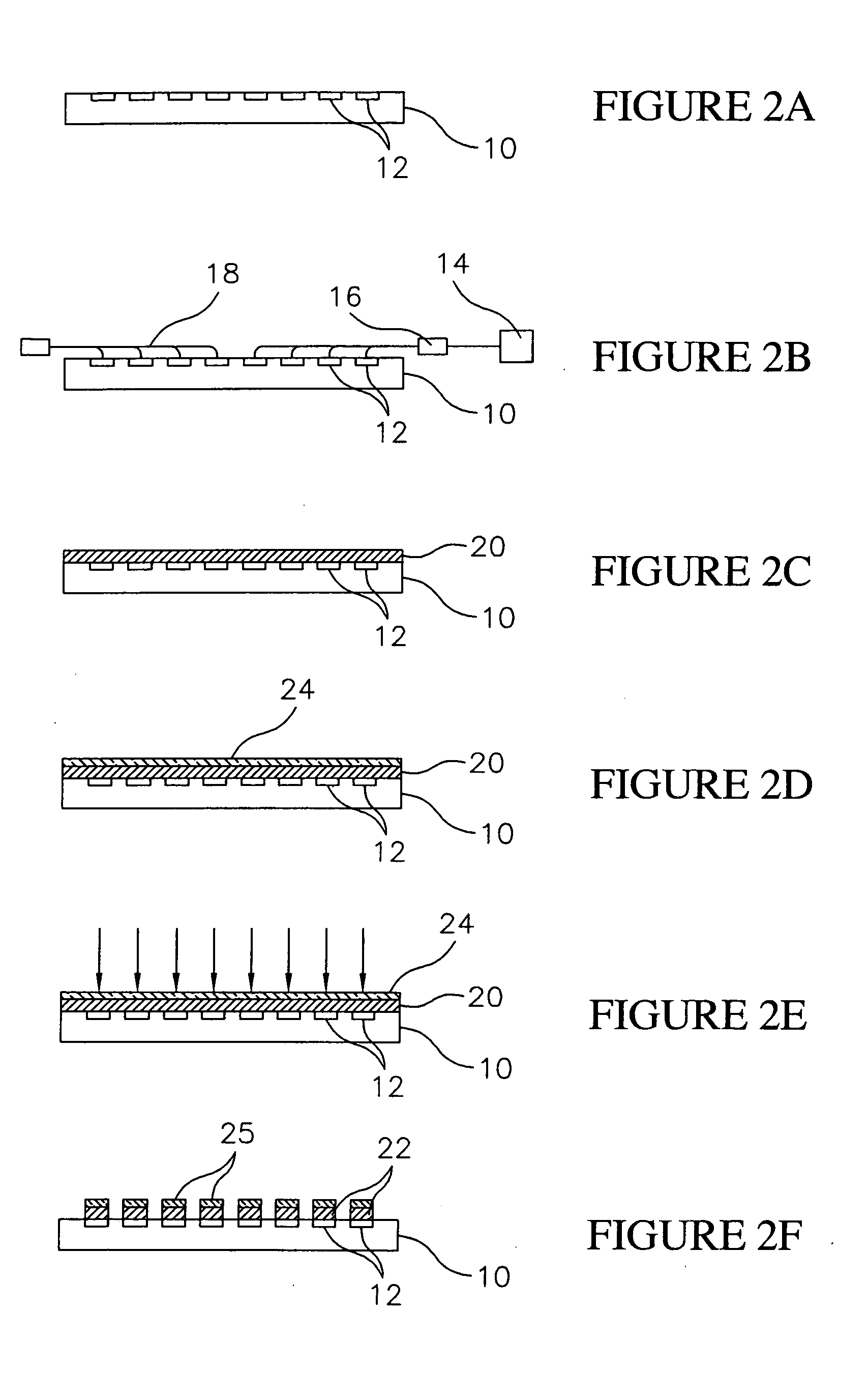
[0028] Referring to FIG. 1, and to FIGS. 2A-2F, broad steps in a method for fabricating semiconductor components in accordance with the invention are illustrated. In the illustrative embodiment the components comprise semiconductor dice, or semiconductor packages (e.g., chip scale packages or minimally packaged dice).

[0029] Initially, as shown in FIG. 2A, a semiconductor substrate 10 containing a plurality of semiconductor components 12 is provided. For example, the substrate 10 can comprise a wafer, or a portion thereof, made of a conventional semiconductor material, such as silicon or gallium arsenide, on which semiconductor dice have been formed using well known processes, such as doping, CVD and etching. As another example, the substrate 10 can comprise a panel containing a plurality of semiconductor packages. In this case the substrate 10 can be made of an organic material, such as a glass filled resin, such as epoxy glass (FR-4), polyimide glass, or a cyanate-glass material. ...


PUM


Abstract

A method for fabricating semiconductor components is performed using a laser scanner and a laser imaging process. A substrate, such as a semiconductor wafer, containing multiple semiconductor components, such as dice or packages, is provided. The components include integrated circuits, and component contacts in electrical communication with the integrated circuits. Initially, the components are tested to identify and locate good components and defective components on the substrate. Using data from the testing step and the laser scanner, patterns of conductors are then formed to either repair the defective components, to electrically isolate the defective components for burn-in, or to form component clusters containing only the good components. Alternately, using data from the testing step and the laser scanner, a matching test board can be fabricated, and used to electrically engage the good components, while the defective components remain isolated.

Description

FIELD OF THE INVENTION [0001] This invention relates generally to semiconductor manufacture and testing, and more particularly to a method for fabricating and testing semiconductor components. BACKGROUND OF THE INVENTION [0002] Photolithography is widely used in semiconductor manufacture and other applications. During photolithography, an exposure energy, such as ultraviolet light, is passed through a mask and onto a target such as a semiconductor wafer. The mask contains opaque and transparent regions which form a primary mask pattern. The exposure energy exposes the mask pattern on a layer of resist deposited on the target. Following exposure, the layer of resist can be developed to form a resist mask. In semiconductor manufacture, such a resist mask can be used for etching, ion implantation, screen printing, CVD and other processes. [0003] One recently developed form of lithography uses a laser scanner to focus modulated laser beams in a series of scan lines onto a radiant sensit...

Claims


Application Information

Patent Timeline
IPC IPC(8): H01L21/66
CPCH01L22/20H01L2924/01087H01L2924/014H01L2224/16H01L24/03H01L24/05H01L2224/05001H01L2224/05022H01L2224/05548H01L2224/05624H01L2224/05647H01L2224/05666H01L2224/0568H01L2224/05681H01L2224/05684H01L2224/0615H01L2924/00014H01L2224/05099H01L2924/013
Inventor HEMBREE, DAVID R.WOOD, ALAN G.
Owner MICRON TECH INC
Why Eureka
Try Eureka