Process for strengthening semiconductor substrates following thinning

Active Publication Date: 2005-04-21
MICRON TECH INC
View PDF15 Cites 52 Cited by
  • Summary
  • Abstract
  • Description
  • Claims
  • Application Information

AI Technical Summary

Benefits of technology

[0035] The advantages of the present invention include the fabrication of a wafer in which warping stresses are counteracted during manufacture and subsequent use of individual semiconductor dice singulated therefrom, wafer backside surface damage due to backgrinding is repaired, very thin wafers of large diameter may be effectively produced at a high yield rate, and polishing of the thinned wafer backside is not required, thus saving substantial time and expense. Furthermore, the layer or film of reinforcement material

Problems solved by technology

A fine polishing act is not requir

Method used


Image

  • Process for strengthening semiconductor substrates following thinning
  • Process for strengthening semiconductor substrates following thinning
  • Process for strengthening semiconductor substrates following thinning

Examples


Embodiment Construction

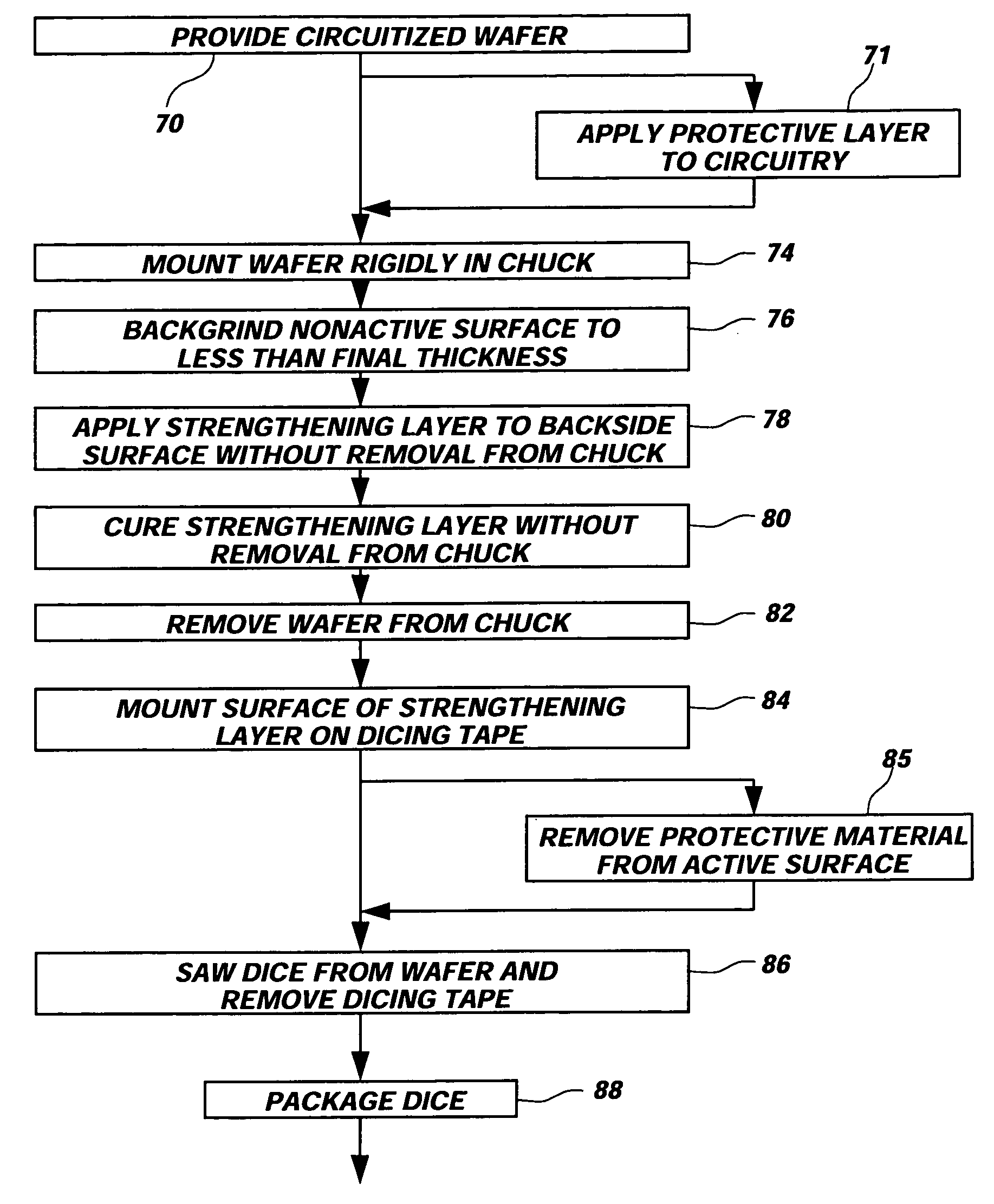
[0051] The general acts in the method of the present invention are shown in FIG. 9. A circuitized wafer 10 having integrated circuitry fabricated on the active surface thereof is provided (act 70).

[0052] In act 74, the wafer 10 is clamped into a fixture, for example, in the form of chuck 60 (see FIG. 10) such that the backside surface 14 is exposed for backgrinding in subsequent act 76. The chuck 60 that is used must be capable of holding and maintaining the wafer 10 in a planar configuration in spite of increasing warping tendencies that may be induced or magnified during grinding. Various wafer chucks 60 in the art are suitable for use. Especially applicable are those which rigidly grip the wafer edge (i.e., edge bead ring EBR) 58 about the circumference, maintaining the wafer in a nonwarping configuration. Another example of a chuck that may be used is described in U.S. Pat. No. 6,279,976 to Ball, assigned to the assignee of the present application, and hereby incorporated herei...


PUM

PropertyMeasurementUnit
Fractionaaaaaaaaaa
Fractionaaaaaaaaaa
Thicknessaaaaaaaaaa

Abstract

A semiconductor wafer having a high degree of thinness and exhibiting an enhanced strength state. A layer of tenacious reinforcement material is disposed over a back side of the wafer while in a rough state from backgrinding, without prior, conventional polishing or plasma etching of the back side. The thin layer or film of reinforcement material fills grooves, fractures and scratches in the back side of the wafer, enhance the rigidity of the wafer and provide a planar, smooth, back side surface layer. The reinforcement material counteracts internal stresses of the wafer tending to warp, crack and propagate lattice defects in the wafer. The reinforcement material may also be configured to act as a die attach adhesive, may provide an ionic barrier, and may remain as part of the packaging for semiconductor dice singulated from the wafer.

Description

BACKGROUND OF THE INVENTION [0001] 1. Field of the Invention[0002] The present invention relates generally to processes and methods for fabricating electronic devices from semiconductor materials. More particularly, the present invention pertains to methods and apparatus offering improved process control for fabricating electronic devices having substrates of reduced thickness and enhanced quality. [0003] 2. State of the Art[0004] The manufacture of semiconductor devices, commonly termed “dice” or “chips,” encompasses a plurality of major manufacturing stages, each of which typically comprises a number of elements. In general, chip manufacture may be generalized as comprising the stages of crystal growth, wafer preparation, wafer fabrication, wafer sort, and packaging. Wafer sort and packaging may be performed in a different order, or combined into a single manufacturing stage. Typically, a wafer of a semiconductor material such as silicon is cut from a large crystal and may have a ...

Claims


Application Information

Patent Timeline
IPC IPC(8): H01L21/00H01L21/06H01L21/30H01L21/44H01L21/46H01L21/68H01L21/78H01L23/00H01L23/28H01L23/31
CPCH01L21/6835H01L21/6836H01L2924/0665H01L2924/014H01L2924/01033H01L2924/01006H01L2224/2919H01L24/27H01L21/78H01L23/3114H01L23/3142H01L23/562H01L24/83H01L2221/68327H01L2221/6834H01L2224/16H01L2224/274H01L2224/83191H01L2224/8385H01L2924/01005H01L2924/01013H01L2924/01029H01L2924/01032H01L2924/01046H01L2924/01049H01L2924/01082H01L2924/01088H01L2924/07802H01L2924/09701H01L2924/14H01L2924/19041H01L2924/19043H01L2924/3511H01L24/29H01L2924/00H01L2924/3512H01L2224/05568H01L2224/05573H01L2924/00014H01L2924/181H01L2224/05599
Inventor DERDERIAN, JAMES M.DRANEY, NATHAN R.
Owner MICRON TECH INC
Why Eureka
Try Eureka