Silicon epitaxial wafer and its production method

a technology of epitaxial wafers and silicon, applied in the direction of polycrystalline material growth, crystal growth process, chemically reactive gases, etc., can solve the problems of reducing the ig capability of epitaxial wafers, small size, and lack of ig capability, so as to improve the resistance to latching and the effect of preventing a change in the resistivity of the epitaxial layer

Inactive Publication Date: 2005-04-28
SHIN-ETSU HANDOTAI CO LTD
View PDF4 Cites 15 Cited by
  • Summary
  • Abstract
  • Description
  • Claims
  • Application Information

AI Technical Summary

Benefits of technology

[0025] While no specific limitation is imposed on the lower limit of resistivity as a substrate for a p / p+ type epitaxial wafer, a boron concentration may be controlled to about 0.014 Ω·cm or higher as a practical crystal pulling condition. However, as one effect of a p+ type substrate for a p / p+ type epitaxial wafer, there is an effect of improving a resistance to latch-up in a device, and hence resistivity of the substrate is necessary to be about 0.1 Ω·cm or lower to obtain the effect, preferably 0.05 Ω cm or lower, and most preferably 0.02 Ω·cm or lower to ensure the sufficient effect.
[0026] On the other hand, with higher resistivity of a substrate, there are obtained an effect of difficulty in generating an OSF ring and in addition thereto an additional effect of no necessity for forming an oxide film on a back surface of a wafer used for preventing a change in resistivity of an epitaxial layer due to auto-doping. While any conditions for a heat treatment for growing Grown-in precipitation nuclei may be adopted as far as Grown-in precipitation nuclei can grow to a size equal to or larger than a value empirically detectable after epitaxial growth, there may be employed such conditions as about 1000° C. or higher and about 0.5 hr or longer. Accordingly, an excellent IG capability can be added all over the radial direction of the wafer at a stage prior to a device process.
[0027] From the above description, according to the present invention, there can be obtained a silicon epitaxial wafer having an excellent gettering capability all over the radial direction of the wafer.

Problems solved by technology

In the case of a usual as-grown wafer, an oxygen precipitation nucleus present at a stage prior to a device process is very small in size and therefore has no IG capability.
Therefore, there has remained a problem to reduce an IG capability of an epitaxial wafer.
Surface distribution in density of Grown-in precipitation nuclei in a substrate prior to an epitaxial step is not necessarily uniform.
If such a substrate is subjected to a heat treatment to grow Grown-in precipitation nuclei and then epitaxial growth is carried out, surface distribution in density of precipitates in an epitaxial wafer becomes non-uniform, leading to a problem of non-uniformity in an IG capability.
Therefore, the problem of non-uniformity of an IG capability in a surface of the substrate as described above easily arises especially in a p / p+ type epitaxial wafer using a p+ type substrate.
In such cases, a problem of non-uniformity in an IG capability arises as in the case of a p+ type substrate.
In such a device process, since there is a case where the sum of the total heat treatments corresponds to only a heat treatment of the order of 2 hours at 1000° C., there cannot be expected growth of oxide precipitates during the device process, which was realized in the prior practice.

Method used


Image

  • Silicon epitaxial wafer and its production method
  • Silicon epitaxial wafer and its production method
  • Silicon epitaxial wafer and its production method

Examples


example 1

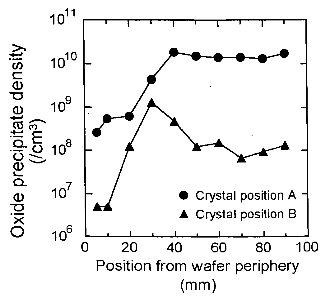
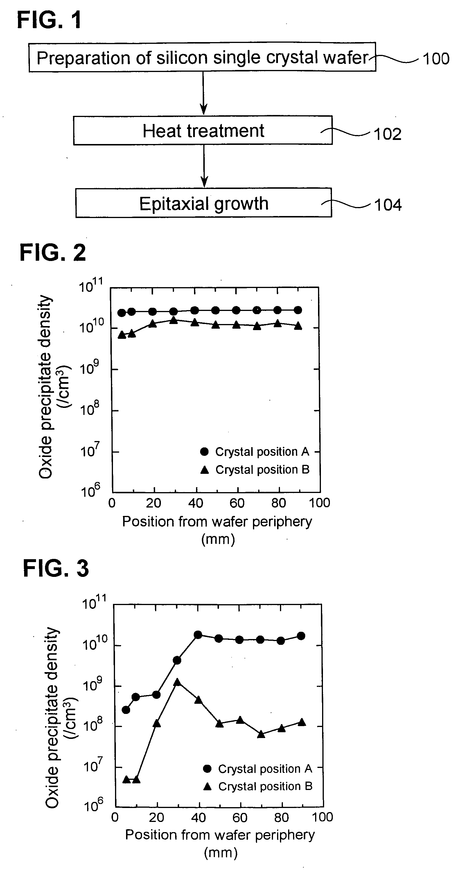
[0043] Mirror-finished substrates were prepared from different two positions (which are positions grown in the former half and the latter half, respectively, in a crystal growth step and hereinafter referred to as a crystal position A and a crystal position B) of a boron-doped silicon single crystal having a diameter of 8 inches, a plane orientation of , and resistivity in the range of from about 0.015 to about 0.018 Ω·cm grown by the CZ method. An oxygen concentration of the substrates which was measured using a gas fusion method was about 14 ppma.

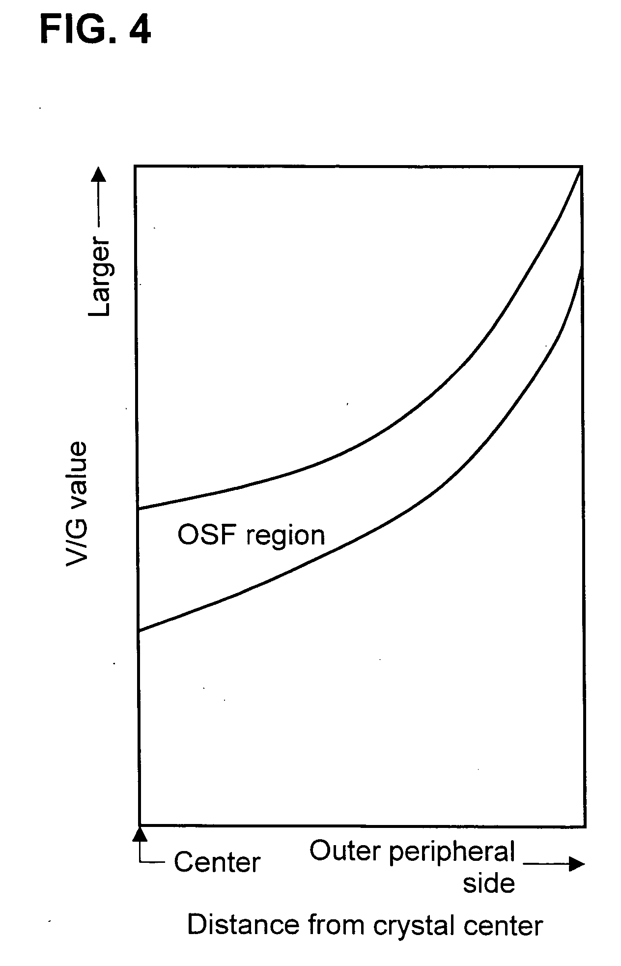
[0044] In pulling of the crystal, a V / G value was adjusted such that an OSF ring is annihilated toward the outer periphery thereof.

[0045] Then, the substrate was subjected to a heat treatment in an oxidizing atmosphere prior to an epitaxial step. That is, the substrate was loaded into a heat treatment furnace at 800° C., the temperature was raised from 800° C. to 1000° C. at a rate of 3° C. / min and the substrate was kept at 1000° C. for...


PUM

PropertyMeasurementUnit
resistivityaaaaaaaaaa
temperatureaaaaaaaaaa

Abstract

The present invention provides a silicon epitaxial wafer having an excellent IG capability all over the radial direction thereof and a process for manufacturing the same. The present invention is directed to a silicon epitaxial wafer having an excellent gettering capability all over the radial direction thereof, wherein density of oxide precipitates detectable in the interior of a silicon single crystal substrate after epitaxial growth is 1×10⁹/cm3 or higher at any position in the radial direction.

Description

TECHNICAL FIELD [0001] The present invention relates to a silicon epitaxial wafer having an excellent gettering capability all over the surface thereof and a process for manufacturing the same. BACKGROUND ART [0002] Most of silicon wafers widely used as substrates to fabricate semiconductor devices have been manufactured from a silicon single crystal grown by a Czochralski (CZ) method. In the silicon single crystal grown by the CZ method, interstitial oxygen is contained at a concentration of about 1018 atoms / cm3 as an impurity. The interstitial oxygen precipitates due to supersaturation in the course of a thermal history from solidification in crystal growth till cooling to room temperature (hereinafter also abbreviated to a crystal thermal history) and in a heat treatment of a fabrication process for a semiconductor device, thereby a precipitate of silicon oxide (hereinafter also referred to as an oxide precipitate or simply a precipitate) being formed. [0003] The oxide precipitat...

Claims


Application Information

Patent Timeline
Patent Type & Authority Applications(United States)
IPC IPC(8): H01L21/322
CPCH01L21/3225H01L21/322
Inventor TAKENO, HIROSHI
Owner SHIN-ETSU HANDOTAI CO LTD
Why Eureka
Try Eureka