Isolation buffers with controlled equal time delays

a buffer and equal time technology, applied in the direction of pulse technique, semiconductor/solid-state device testing/measurement, instruments, etc., can solve the problems of significant attenuation of signals on other lines, inability to route multiple lines, and add delay to signals, etc., to achieve significant cost of a tester

Inactive Publication Date: 2005-04-28
FORMFACTOR INC
View PDF8 Cites 26 Cited by
  • Summary
  • Abstract
  • Description
  • Claims
  • Application Information

AI Technical Summary

Benefits of technology

[0015] In accordance with the present invention, circuitry is provided to keep the delay through multiple isolation buffers constant. Providing branching using isolation buffers having equal delays allows creation of an efficient wafer test system, and further allows creation of other systems requiring branch isolation while maintaining equal line delays.
[0016] To prevent isolation buffers from introducing an uncertain delay into the transmission of a signal on multiple lines, in one embodiment buffer delay is controlled by varying the power supply voltage potential provided to the isolation buffers. Alternatively, the buffer delay can be adjusted by controlling current, such as by controlling current through an isolation buffer configured as a differential amplifier.
[0019] In a further embodiment to reduce circuitry required relative to using two buffers in each branch, an isolation buffer with its delay controlled by the delay control circuit is provided in a channel prior to the branch point. Buffers without delay control having fixed system output voltages are then provided in each branch point. The reference buffer in the delay control circuit is then made up of two buffers, one having its delay controlled to match the variable delay isolation buffers, while the second has no delay control so it supplies a fixed system output voltage and matches the buffers provided in each branch.
[0020] For a wafer test system, simply changing a probe card to one having channels branched through equal delay isolation buffers made in accordance with the present invention allows a tester with a limited number of channels to test all ICs on a wafer. With such branching the prober does not need repositioning to contact the wafer a number of times, as would be required without using branches in the probe card. The cost of a tester is significant relative to the cost of a probe card, so although modifying the tester to include the delay isolation buffers is possible, simply substituting probe cards with the isolation buffers will be a significantly less expensive alternative.

Problems solved by technology

In some cases, however, it may be impossible to route the multiple lines so that all are the same length.
Further, a fault or line degradation may occur on one of the multiple lines that can create a return signal causing interference and significant attenuation of signals on other lines.
Unfortunately, the isolation buffer circuitry will not only add delay to the signals, but it will typically introduce an arrival delay uncertainty, or effectively create phase differences at the destination of the multiple transmission lines.
Circuit construction variations and temperature variations are typical contributors to delay variations from one buffer circuit to another that can prove problematic to synchronous circuits.
Although one channel can be fanned out, with fan out a fault identified in test results provided from one DUT may falsely appear in the test results of another DUT.
For example a fault in the contact pad on one DUT which is shorted to ground will short the contact pad on a second DUT to ground, causing the second DUT to falsely test as bad.
Further, an open circuit fault on one of the lines will render a wafer connected to the line untestable.
Either a short or an open on a line will severely attenuate a test signal provided from the same channel to other lines intended for other DUTs.
Although reducing the affect of faults, isolation resistors do not completely eliminate the attenuation caused by the faults.
Further, with a parasitic capacitance on the lines, adding isolation resistors introduces an RC delay that can adversely affect the rise and fall time of test signals, potentially creating erroneous test results.
The delay is uncertain because the delay through a buffer can change with changes in temperature and power supply voltage.
The signal delay from the tester to DUTs on a wafer can change during performance of a sequence of tests on DUTs of a wafer, creating inaccurate test results.

Method used


Image

  • Isolation buffers with controlled equal time delays
  • Isolation buffers with controlled equal time delays
  • Isolation buffers with controlled equal time delays

Examples


Embodiment Construction

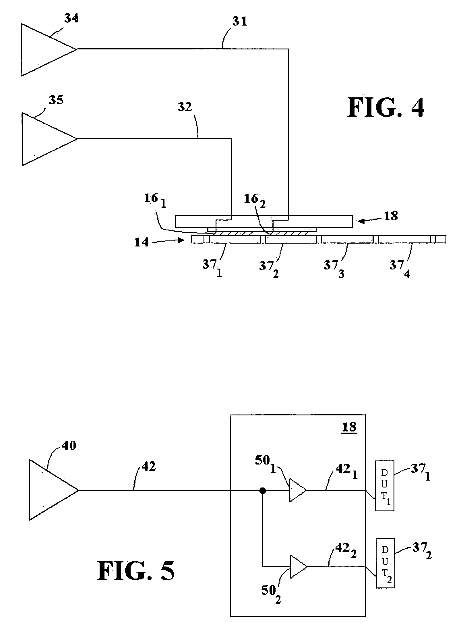
[0035]FIG. 6 shows an embodiment of the isolation buffer 50 with delay control which can change the bias voltage supplied to the buffer 50. In FIG. 6, the buffer 50 includes an inverter 51 having a signal input 55 and output 56. The system power supply voltage rails 57 and 58 carry a high voltage V+ and a low voltage V−. With CMOS devices, the bias or power supply voltages are typically referred to as Vdd and Vss. Typically, the rail voltages V+ and V− are supplied directly to the buffer. The voltage V+, for example, may be 5 volts, while V− may be ground or zero volts. However, in FIG. 6 with the delay control circuit set to control delay by varying power supply voltage, the voltage rails V+ and V− are provided through respective delay control circuits 60 and 61 as the high and low power supply voltages to inverter 51. Although shown as two separate delay control circuits 60 and 61 in FIGS. 5 and 6, a single combined circuit can be used. Further, although two circuits 60 and 61 are...


PUM


Abstract

A system is provided for controlling the delay in an isolation buffer. Multiple such isolation buffers are used to connect a single signal channel to multiple lines and controlled to provide an equal delay. Isolation buffer delay is controlled to be uniform by varying either power supply voltage or current. A single delay control circuit forming a delay-lock loop supplies the delay control signal to each buffer to assure the uniform delay. Since controlling delay can also vary the output voltage of each isolation buffer, in one embodiment buffers are made from two series inverters: one with a variable delay, and the second without a variable delay providing a fixed output voltage swing. To reduce circuitry needed, in one embodiment an isolation buffer with a variable power supply is provided in a channel prior to a branch, while buffers having a fixed delay are provided in each branch. A wafer test system can be configured using the isolation buffers having equal delays to enable concurrently connecting one tester channel to multiple wafer test probes.

Description

BACKGROUND [0001] 1. Technical Field [0002] The present invention relates in general to distributing a signal to multiple lines through isolation buffers to prevent signal degradation. More particularly, the present invention relates to a system for connecting a single test signal channel of a wafer test system to multiple test probes to enable testing of integrated circuits (ICs) on a wafer. [0003] 2. Related Art [0004] Fanning out a signal to multiple transmission lines, as illustrated in FIG. 1, in many cases requires that the signal arrive at multiple destinations with an equal phase shift. For example to fan out a clock signal, a clock tree is used to distribute the clock signal so that signals arriving on multiple lines are synchronized, or distributed without a phase difference at the line destinations. Typically to assure no phase difference, the multiple transmission lines are laid out to have the same length. In some cases, however, it may be impossible to route the multip...

Claims


Application Information

Patent Timeline
Patent Type & Authority Applications(United States)
IPC IPC(8): G01RG01R1/00G01R31/02G01R31/26H03H11/12H03H11/26H03K3/00
CPCG01R31/2889H03H11/265H03H11/126G01R31/31917G01R31/26H01L22/00H03K5/13
Inventor MILLER, CHARLES A.
Owner FORMFACTOR INC
Why Eureka
Try Eureka